


— 5 —
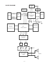
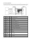
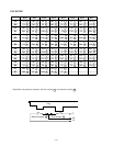
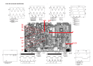
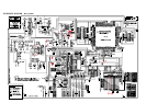
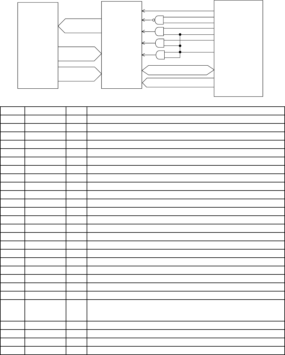
KEY TOUCH LSI(HG52E35P)
By counting the time between the first key input signal FI and the second SI from the keyboard unit, the key
touch LSI detects key velocity of 256-step. Then the LSI sends the CPU note numbers and their velocities.
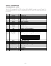
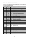
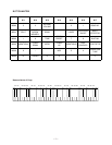
Pin No. Terminal In/Out Function
1 REQB Out Interrupt request. Not used.
2,3 FI10,SI10 In Connected to +5V.
4 VCC In +5V source.
5 CRDB In Read enable signal.
6 CWRB In Write enable signal.
7 CCBB In Chip select signal.
8 T In Test terminal. Connected to +5V.
9 STYB In Standby terminal. Connected to +5V.
10 RESB In Reset signal.
11 W In Test terminal. Connected to +5V.
12 CKI In External clock input.
13 TMD In Test terminal. Connected to ground.
14 TST In Test terminal. Connected to ground.
15 CKO Out External clock output. Not used.
16 GND In Ground(0V) source.
17 XIN In Clock pulse input. Connected to ground.
18 XOUT Out Clock pulse output. Not used.
19 TRES In Test terminal. Connected to ground.
20~28 CD0~CD7 In/Out Data bus.
24 GND In Ground(0V) source.
29~31 CA0~CA2 Out Address bus.
32 VCC In +5V source.
33~4333~43
53~5553~55
57~6357~63
FI0~FI9FI0~FI9
SI0~SI9SI0~SI9
In Key input signal.
40 VCC In +5V source.
44~53 KC0~KC7 Out Key scan signal.
48,56 GND In Ground(0V) source.
54 VCC In +5V source.
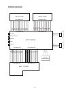
Keyboard
KC0~KC7
FI0~FI9
SI0~SI9
Key Touch LSI
HG52E35P
RESB
CCSB
CWRB
CRDB
CKI
P30/D0~P37/D7
P12/A2~P10/A0
CA0~CA2
CD0~CD7
D0~D7
A0~A2
CPU
HD6433298A16P
P52/SCK
A12
A14
P44/-WR
P42/IRQ0
P43/-RD
P46/PHI