2002 May 22 11
Philips Semiconductors Product specification
Low power audio DAC UDA1334BT
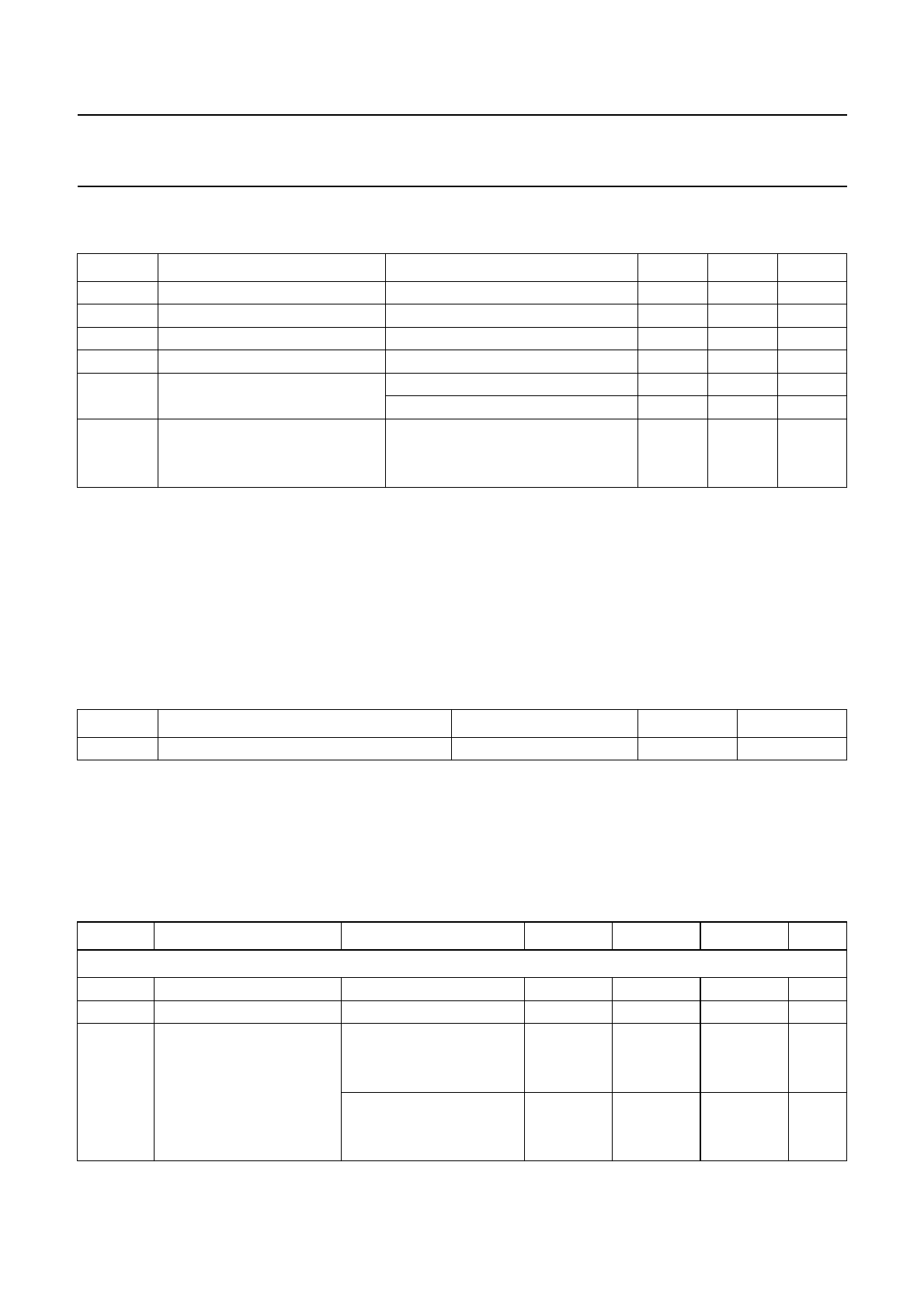
9 LIMITING VALUES
In accordance with the Absolute Maximum Rating System (IEC 60134).
Note
1. All supply connections must be made to the same power supply.
2. Short-circuit test at T
amb
=0°C and V
DDA
= 3 V. DAC operation after short-circuiting cannot be warranted.
10 HANDLING
Inputs and outputs are protected against electrostatic discharge in normal handling. However, it is good practice to take
normal precautions appropriate to handling MOS devices.
11 THERMAL CHARACTERISTICS
12 QUALITY SPECIFICATION
In accordance with
“SNW-FQ-611-D”
.
13 DC CHARACTERISTICS
V
DDD
=V
DDA
= 2.0 V; T
amb
=25°C; R
L
=5kΩ; all voltages with respect to ground (pins V
SSA
and V
SSD
); unless
otherwise specified.
SYMBOL PARAMETER CONDITIONS MIN. MAX. UNIT
V
DD
supply voltage note 1 − 4.0 V
T
xtal(max)
maximum crystal temperature − 150 °C
T
stg
storage temperature −65 +125 °C
T
amb
ambient temperature −40 +85 °C
V
es
electrostatic handling voltage human body model −2000 +2000 V
machine model −200 +200 V
I
sc(DAC)
short-circuit current of DAC note 2
output short-circuited to V
SSA
− 450 mA
output short-circuited to V
DDA
− 300 mA
SYMBOL PARAMETER CONDITIONS VALUE UNIT
R
th(j-a)
thermal resistance from junction to ambient in free air 145 K/W
SYMBOL PARAMETER CONDITIONS MIN. TYP. MAX. UNIT
Supplies
V
DDA
DAC analog supply voltage note 1 1.8 2.0 3.6 V
V
DDD
digital supply voltage note 1 1.8 2.0 3.6 V
I
DDA
DAC analog supply current normal operating mode
at 2.0 V supply voltage − 2.3 − mA
at 3.0 V supply voltage − 3.5 − mA
Sleep mode
at 2.0 V supply voltage − 125 −µA
at 3.0 V supply voltage − 175 −µA


