


— 5 —
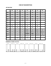
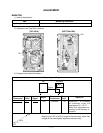
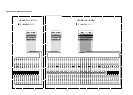
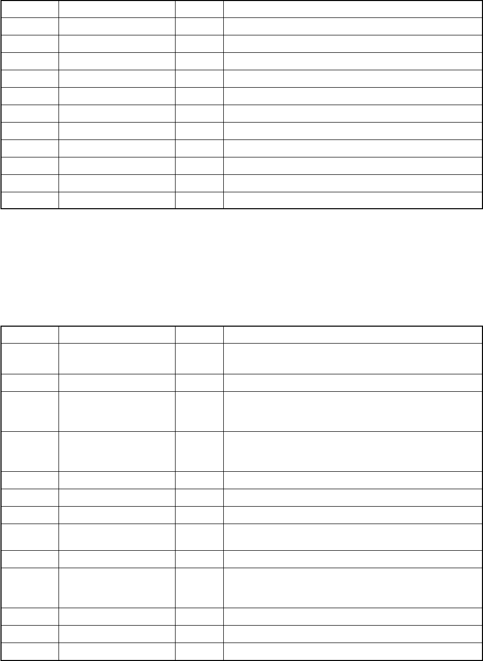
Pin No. Terminal In/Out Function
74 ~ 77 DB4 ~ DB7 Out Data bus for the LCD driver
78 NC9 — Not used
79 LVCC In +5 V source
80 ~ 84 KO8 ~ KO12 Out Terminals for button scan signal
85 ~ 87 P65 ~ P67 — Not used
88 RS Out Control signal for the LCD driver
89 R/W Out Read/Write signal for the LCD driver
90 E Out Chip enable signal for the LCD driver
91 ~ 95 P73 ~ P77 — Not used
96 LGND In Ground source
97, 100 MA18, MA15 Out Address bus
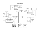
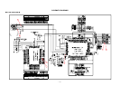
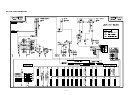
LCD DRIVER (LSI3: KS0066U-10B)
The LCD driver can drive a dot matrix LCD having 40 segment and 16 common lines. The LSI contains 240
graphic symbols in the built-in character generator ROM, and stores 80 characters in the built-in display data
RAM. In accordance with command from the CPU, the LSI is capable of displaying up to 16 characters
simultaneously. The following table shows the pin functions of LSI3.
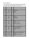
Pin No. Terminal In/Out Function
1 ~ 22,
SEG1 ~ SEG40 Out Segment signal output
63 ~ 80
23 VSS — GND (0 V) source
Terminals for the built-in clock pulse generator. The
24, 25 OSC1, OSC2 In/Out external resistor connected determines the oscillation
frequency.
LCD drive voltage input.
26 ~ 30 V1 ~ V5 In Those voltages are used for generating the stepped
pulse of the LCD drive signals.
31, 32 LP, XCLS — Not used
33 VDD In DVDD (+5 V) source
34, 35 FR, DO — Not used
36 RS In
Data/command determination terminal.
High: data, Low: command
37 R/W In Read/Write terminal. High: read, Low: write
Chip enable signal.
38 E In High: enable, the writing is done at fall edge.
Low: disenable
39 ~ 42 DB0 ~ DB3 — Not used. Connected to GND (0 V)
43 ~ 46 DB4 ~ DB7 In/Out Data bus
47 ~ 62 COM1 ~ COM16 Out Common signal/output