


— 7 —
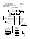
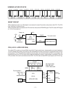
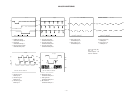
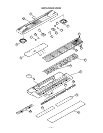
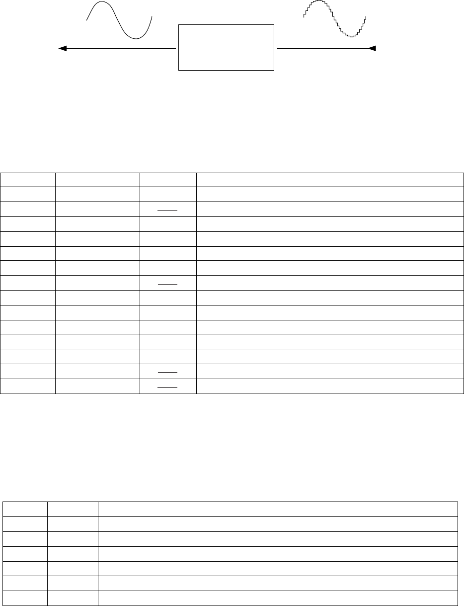
Filter Block
From DAC
To power amplifier
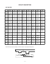
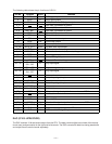
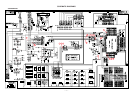
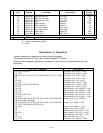
Name Voltage For operation of
VDD +5 V CPU, Reset IC, Sound source ROM, LED Latches
DVDD +5 V Power jack, Photocoupler
AVDD +5V DAC, Filter
LVDD +5 V LED Drivers
VCC +9 V Power amplifier, Pilot lamp
VC +9 V Power amplifier
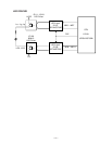
Pin No. Terminal In/Out Function
1 Power GND In Ground (0V) source
2 Ch1 B.S. Terminal for a bootstrap capacitor
3 Ch1 OUT Out Channel 1 output
4 VCC In +9V source
5 Ch1 N.F. In Negative feedback input
6 Ch1 IN In Channel 1 input
7 D.C. Terminal for a decoupling capacitor
8 Pre GND In Ground (0V) source
9 Stand by In Power control signal input. 0 V: Off, +9 V: On
10 Ch2 IN In Channel 2 input
11 Ch2 N.F. In Negative feedback input
12 Ch2 OUT Out Channel 2 output
13 Ch2 B.S. Terminal for a bootstrap capacitor
14 NC Not used
POWER SUPPLY CIRCUIT
The power supply circuit generates six voltages as shown in the following table. VDD voltage is always
generated. The others are controlled by APO signal from the CPU.
FILTER BLOCK
Since the sound signals from the DAC are stepped waveforms, the filter block is added to smooth the
waveforms.
POWER AMPLIFIER (IC102: LA4598)
The power amplifier is a two-channel amplifier with standby switch.
The following table shows the pin function of IC102.