


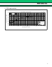
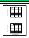
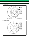

MB15E07SL
13
■
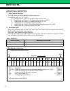
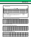
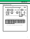
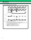
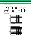
SERIAL DATA INPUT TIMING
1st data
2nd data
Control bit Invalid data
Data
Clock
LE
MSB LSB
t
1 t2 t3
t6
t5t4
t7
∼
∼
∼
∼
Note : LE should be “L” when the data is transferred into the shift register.
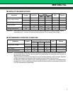
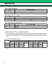
Parameter Min Typ Max Unit
t
1 20 – – ns
t
2 20 – – ns
t3 30 – – ns
t4 30 – – ns
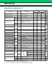
Parameter Min Typ Max Unit
t
5 100 – – ns
t
6 20 – – ns
t7 100 – – ns
On the rising edge of the clock, one bit of data is transferred into the shift register.