


MB15E07SL
3
■
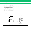
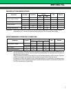
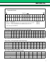
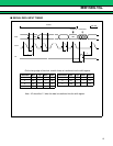
PIN DESCRIPTIONS
Pin no.
Pin
name
I/O Descriptions
SSOP BCC
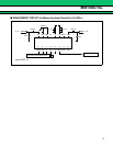
116OSC
IN I Programmable reference divider input. Connection to a TCXO.
21OSC
OUT O Oscillator output.
32V
P – Power supply voltage input for the charge pump.
43VCC – Power supply voltage input.
54D
O O
Charge pump output.
Phase of the charge pump can be selected via programming of the FC bit.
6 5 GND – Ground.
7 6 Xfin I Prescaler complementary input, which should be grounded via a capacitor.
87finI
Prescaler input.
Connection to an external VCO should be done via AC coupling.
98ClockI
Clock input for the 19-bit shift register.
Data is shifted into the shift register on the rising edge of the clock.
(Open is prohibited.)
10 9 Data I
Serial data input using binary code.
The last bit of the data is a control bit. (Open is prohibited.)
11 10 LE I
Load enable signal input. (Open is prohibited.)
When LE is set high, the data in the shift register is transferred to a latch
according to the control bit in the serial data.
12 11 PS I
Power saving mode control. This pin must be set at “L” at Power-ON.
(Open is prohibited.)
PS = “H”; Normal mode
PS = “L”; Power saving mode
13 12 ZC I
Forced high-impedance control for the charge pump (with internal pull up
resistor.)
ZC = “H”; Normal Do output.
ZC = “L”; Do becomes high impedance.
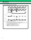
14 13 LD/fout O
Lock detect signal output (LD)/phase comparator monitoring output (fout).
The output signal is selected via programming of the LDS bit.
LDS = “H”; outputs fout (fr/fp monitoring output)
LDS = “L”; outputs LD (“H” at locking, “L” at unlocking.)
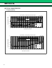
15 14 φPO
Phase comparator N-channel open drain output for an external charge
pump. Phase can be selected via programming of the FC bit.
16 15 φRO
Phase comparator CMOS output for an external charge pump. Phase can
be selected via programming of the FC bit.