


MB15F74UV
3
■
■■
■
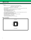
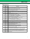
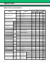
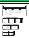
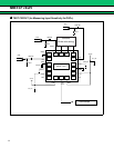
PIN DESCRIPTION
Pin no.
Pin
name
I/O Descriptions
1GND Ground pin for OSC input buffer and the shift register circuit.
2fin
IF I
Prescaler input pin for the IF-PLL.
Connection to an external VCO should be AC coupling.
3Xfin
IF I
Prescaler complimentary input for the IF-PLL section.
This pin should be grounded via a capacitor.
4GNDIF Ground pin for the IF-PLL section.
5V
CCIF
Power supply voltage input pin for the IF-PLL section, the shift register and the oscillator
input buffer.
6Do
IF O Charge pump output for the IF-PLL section.
7PSIF I
Power saving mode control pin for the IF-PLL section. This pin must be set at “L” when
the power supply is started up. (Open is prohibited.)
PS
IF = “H” ; Normal mode/PSIF = “L” ; Power saving mode
8 LD/fout O
Lock detect signal output (LD) /phase comparator monitoring output (fout) pin. The out-
put signal is selected by LDS bit in a serial data.
LDS bit = “H” ; outputs fout signal/LDS bit = “L” ; outputs LD signal
9PS
RF I
Power saving mode control for the RF-PLL section. This pin must be set at “L” when the
power supply is started up. (Open is prohibited. )
PS
RF = “H” ; Normal mode/PSRF = “L” ; Power saving mode
10 DoRF O Charge pump output for the RF-PLL section.
11 V
CCRF Power supply voltage input pin for the RF-PLL section.
12 GND
RF Ground pin for the RF-PLL section
13 Xfin
RF I
Prescaler complimentary input pin for the RF-PLL section.
This pin should be grounded via a capacitor.
14 finRF I
Prescaler input pin for the RF-PLL.
Connection to an external VCO should be via AC coupling.
15 LE I
Load enable signal input pin (with the schmitt trigger circuit)
When LE is set “H”, data in the shift register is transferred to the corresponding latch ac-
cording to the control bit in a serial data.
16 Data I
Serial data input pin (with the schmitt trigger circuit)
Data is transferred to the corresponding latch (IF-ref. counter, IF-prog. counter,
RF-ref. counter, RF-prog. counter) according to the control bit in a serial data.
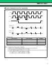
17 Clock I
Clock input pin for the 23-bit shift register (with the schmitt trigger circuit)
One bit data is shifted into the shift register on a rising edge of the clock.
18 OSC
IN I
The programmable reference divider input pin. TCXO should be connected with an AC
coupling capacitor.