


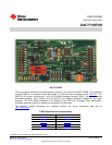

www.ti.com
Analog Interface
2 Analog Interface
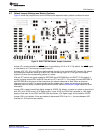
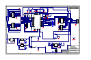
For maximum flexibility, the DAC7716EVM can interface to multiple analog sources. Samtec part numbers
SSW-110-22-F-D-VS-K and TSM-110-01-T-DV-P provide a 10-pin, dual-row, header at J1. This header
provides access to the analog input and output pins of the DAC. Consult Samtec at
http://www.samtec.com or call 1-800-SAMTEC-9 for a variety of mating connector options.
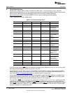
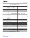
Table 1 summarizes the pinouts for analog interface J1.
Table 1. J1: Analog Interface Pinout
Pin Number Signal Description
J1.1 SGND-0 Signal GND DAC output 0
J1.2 V
OUT
-0 Analog output 0
J1.3 SGND-1 Signal GND DAC output 1
J1.4 V
OUT
-1 Analog output 1
J1.5 SGND-2 Signal GND DAC output 2
J1.6 V
OUT
-2 Analog output 2
J1.7 SGND-3 Signal GND DAC output 3
J1.8 V
OUT
-3 Analog output 3
J1.9-13 (odd) AGND Analog ground connections
J1.10 A
IN
Auxiliary analog input
J1.14 V
MON_BUF
Monitor output after buffer
J1.15 Unused —
J1.17-19 (odd) AGND Analog ground connections
J1.18 RefGND Reference ground pins on the
DAC7716 (see below)
J1.20 EXTREF+ External reference source input (+
side of reference input)
J1.12 Unused —
J1.16 Unused —
The analog interface is populated on the top of the evaluation model. This configuration makes it possible
to stack multiple EVMs to run them in daisy-chain mode. J4 can be installed with a 90-degree connector to
allow access to the analog outputs if multiple EVMs are stacked. The J1B connector can be installed if the
part is used as a standalone board.
The DAC7716 can be configured with an output gain of 2 or 4. By default, the analog outputs of the
DAC7716EVM are configured with a gain of 4. If a gain of 2 is desired, the proper jumper must be
installed (JP2-JP5, depending on the output channel), and the command register must be set accordingly.
The SGND pins of the DAC7716 are connected to the ground of the evaluation board.
The Auxiliary Analog Input pin can be further protected from over-voltage and over-driving conditions. A
Schottky diode (D1) can be installed to protect the DAC7716 from an input over-voltage condition. An op
amp buffer is placed on the V
MON
output to limit the current that passes through the pin.
The DAC7716EVM has an external reference voltage option. If an external reference voltage is used,
switches S2 and S3 must be properly configured. Use the EXTREF+ (J1.20) to apply an external
reference voltage.
The DAC7716 is designed to have the REFGND-A and REFGND-B pins within 0.3V of the AGND.
Therefore, we recommend not using the RefGND pin when connecting an external reference. Connect the
ground source of the reference voltage to the ground of the board (J1.19). See the Reference Voltage
section for more information.
3 Digital Interface
The DAC7716EVM is a serial input data converter. The evaluation module is designed for interfacing to
multiple control platforms.
3
SBAU159–October 2009 DAC7716EVM
Submit Documentation Feedback
Copyright © 2009, Texas Instruments Incorporated