


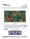
Digital Interface
www.ti.com
3.1 Serial Data Interface
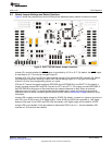
Samtec part numbers SSW-110-22-F-D-VS-K and TSM-110-01-T-DV-P provide a 10-pin, dual-row,
header/socket combination at J2. This header/socket provides access to the digital control and serial data
pins from both J2A (top side) and J2B (bottom side) of the connector. Consult Samtec at
http://www.samtec.com or call 1-800-SAMTEC-9 for a variety of mating connector options.
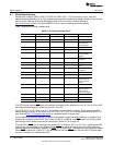
Table 2 describes the serial interface pins.
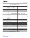
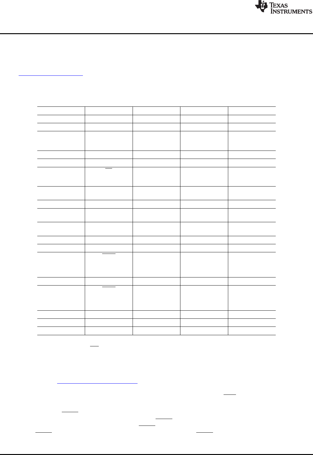
Table 2. J2: Serial Interface Pins
(1)
Pin No. Signal Name I/O Type Pullup Function
J2.1 Unused — —
J2.2 GPIO-0 In/Out High GPIO-0
J2.3 J2.5 SCLK In None DAC7716 SPI
clock; pins are
shorted together
J2.4 DGND In/Out None Digital ground
J2.6 GPIO-1 In/Out High GPIO-1
J2.7 J2.9 CS In None SPI bus chip select;
pins are shorted
together
J2.8 Uni/Bip A In High Output mode select
of Group A
J2.10 DGND In/Out None Digital ground
J2.11 SDO/SDI In/Out None DAC7716 SPI data
in/out
J2.12 Uni/Bip B In High Output mode select
of Group B
J2.13 Unused — —
J2.14 RST In High Input register reset
J2.15 LDAC In High GPIO signal to
control LDAC for
DAC output latch
update
J2.16 Unused — —
J2.17 LDAC In High Alternate GPIO
signal to control
LDAC for DAC
output latch update
J2.18 DGND In/Out None Digital ground
J2.19 Unused — —
J2.20 Unused — —
(1)
Group A contains V
OUT
-0 and V
OUT
-1. Group B contains V
OUT
-2 and V
OUT
-3.
The SCLK signal and the CS signal can each be controlled by two different pins on J2. Pins J2.3 and J2.5
have been shorted together, as well as pins J2.7 and J2.9.
Pins J2.8, J2.12, J2.14, J2.15, and J2.17 have weak pull-up/pulldown resistors. These resistors provide
default settings for many of the control pins. J2.3, J2.5, J2.7, J2.9, J2.11 correspond directly to DAC7716
pins. See the DAC7716 product data sheet for complete details on these pins.
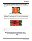
Control signals to and from the DAC7716 can be accessed through the digital interface, or switches and
jumpers found directly on the EVM. The /LDAC, Uni/Bip A, Uni/Bip B, and RST signals are initially pulled
high through 10kΩ resistors and can be controlled by switch S1 or through J2.
The load DAC (LDAC) pin is connected via jumper JP1 to either the J2.15 or J2.17 pin. Updating the DAC
registers can be completed in two different ways. LDAC can either be tied to ground, in which case the
input registers are immediately updated, or LDAC can be pulled high. Therefore, the DAC registers update
when LDAC is taken low. Switch S1.1 can be closed to hold the LDAC low. See the DAC7716 data sheet
for more information on updating the DAC.
4
DAC7716EVM SBAU159–October 2009
Submit Documentation Feedback
Copyright © 2009, Texas Instruments Incorporated