


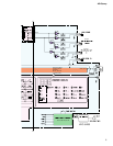
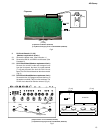
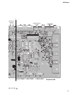
AG-Stomp
17
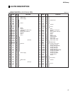
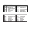
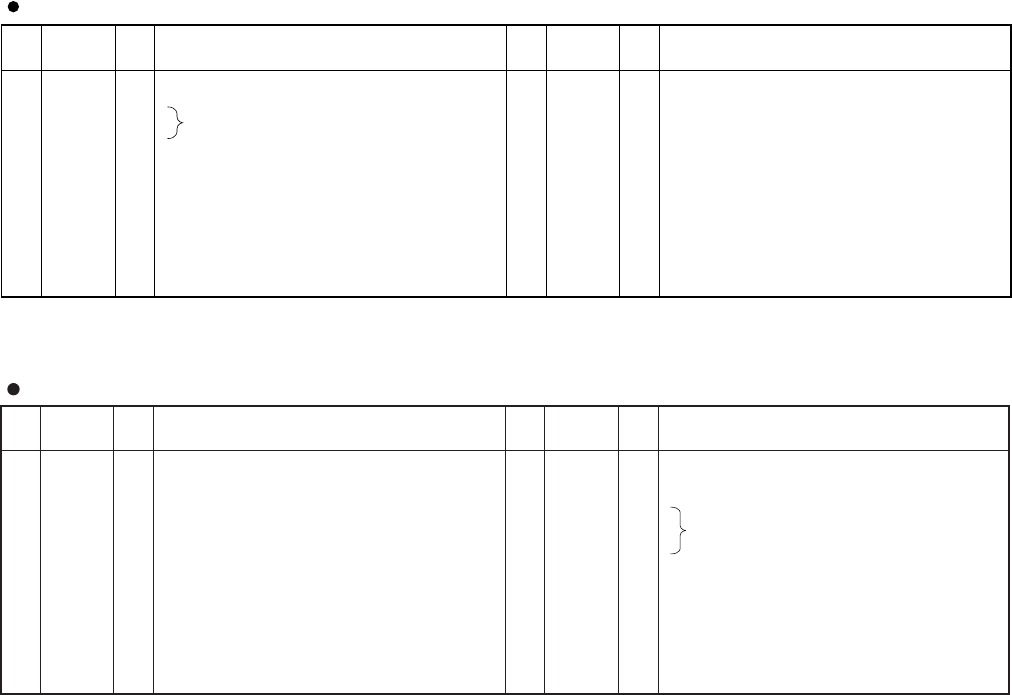
PIN
NO.
I/O FUNCTIONNAME
PIN
NO.
I/O FUNCTIONNAME
1
2
3
4
5
6
7
8
Vss
MCLK
DM0
DM1
RES
WCIN
DIN
V
DD
I
I
I
I
I
I
Ground
Master clock input
DIN/BCLK/WCLK format select
DM1,DM0=0,0 DSP,LDSP (64 bit,LSB first)
DM1,DM0=0,1stereo,DSP (64 bit,MSB first)
DM1,DM0=1,0 DSP2 (128 bit,MSB first)
DM1,DM0=1,1 BB (64 bit,MSB first)
System reset
Word clock input
Digital audio serial data input
Power supply (+5 V)
9
10
11
12
13
14
15
16
MUTE
VFL
CCK
CIN
CLD
CNTR
CSM
DOUT
I
I
I
I
I
I
I
O
Mute
Validity flag
C,U bit clock input/C bit data input
C,U bit data input/U bit data input
End of C,U bit input/16,20 bit/24 bit select
32 bit counter reset/Top of block
Channel status input mode select
CSM=0 Asynchronous mode
CSM=1 Synchronous mode
Digital interface formatted data output
YM3437C-F (XM530A00) DIT2 (Digital Format Interface Transmitter)
DM: IC17
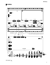
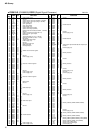
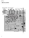
PIN
NO.
1
2
3
4
5
6
7
8
9
10
11
12
13
14
I/O
I
I
I
I
I
I
-
-
I
I
I
I
I
O
VREFH
VREFL
AINR+
AINR-
AINL+
AINL-
VA
AGND
DIF0
DIF1
LRCK
SCLK
SDTI
SDTO
NAME
Positive Voltage Reference Input, VA
Negative Voltage Reference Input, AGND
Rch Analog Positive Input
Rch analog Negative Input
Lch Analog Positive Input
Lch analog Negative Input
Analog Power Supply
Analog Ground
Audio Data Interface Format
Audio Data Interface Format
Input/Output Channel Clock
Audio Serial Data Clock
Audio Serial Data Input
Audio Serial Data Output
FUNCTION
PIN
NO.
15
16
17
18
19
20
21
22
23
24
25
26
27
28
I/O
I
I
I
I/O
I/O
I
-
-
I
I
I
O
O
O
MCLK
DEM0
DEM1
TST3
TST2
TST1
VD
DGND
/PWDA
/PWAD
CMODE
AOUTL
AOUTR
VCOM
NAME
Master Clock Input
De-emphasis Frequency Select
De-emphasis Frequency Select
Test Pins (Pull Down Pins)
Digital Power Supply
Digital Ground
DAC power-Down Mode
ADC power-Down Mode
Master Clock Select (“H”:384 fs,“L”:256 fs)
Lch Analog Output
Rch Analog Output
Common Voltage Output, VA/2
FUNCTION
AK4520A-VF-E2 (XT802A00) DAC & ADC
DM: IC104