KP915GV Product Manual
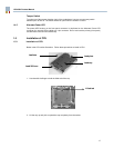
8
Figures
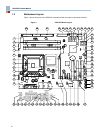
Figure 1. KP915GV Board Layout.............................................................................................12
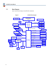
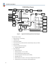
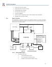
Figure 2. KP915GV Block diagram ...........................................................................................14
Figure 3. Jumpers .....................................................................................................................15
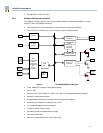
Figure 4. Clocking Block Diagram.............................................................................................25
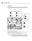
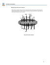
Figure 5. KP915GV Board Slot Layout......................................................................................28
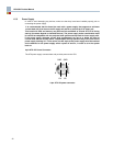
Figure 6. Audio Jack Socket and ATAPI Connectors................................................................29
Figure 7. SST 49LF004B Functional Block Diagram.................................................................38
Figure 8. SigmaTel STAC9200 High Definition Block Diagram.................................................40
Figure 9. NS LM96000CIM Block Diagram ...............................................................................41
Figure 10. PC8374K Block Diagram ...........................................................................................43
Figure 11. BIOS ROM Addresses .............................................................................................110
Tables
Revision history .................................................................................................................................3
Safety and approval notices ..............................................................................................................4
Product Specification Overview.......................................................................................................10
Table 1. KP915GV Motherboard ...................................................................................................26
Table 3. ACPI Power States..........................................................................................................30
Table 4. Power Supply Connector.................................................................................................32
Table 5. Environmental Specifications...........................................................................................33
Table 6. Regulatory Testing*.........................................................................................................34
Table 7. References ....................................................................................................................105
Table 8. I/O Map..........................................................................................................................106
Table 9. PCI Interrupt Allocation..................................................................................................107
Table 10. PCI Device Assignments.............................................................................................108
Table 11. SMBus Resource Allocation ........................................................................................108
Table 12. ISA Interrupt Allocation................................................................................................109
Table 13. ISA DMA Channel Allocation.......................................................................................109
Table 14. Connector part numbers..............................................................................................116
Table 15. ADD2 Expansion Slot ..................................................................................................117
Table 16. PCI Expansion Slot......................................................................................................118
Table 17. PCI Express x1 Slot (PCI-E x1)...................................................................................119
Table 18. P/S2 Mouse and P/S2 Keyboard.................................................................................119
Table 20. Serial Port....................................................................................................................120
Table 21. VGA Port .....................................................................................................................120
Table 22. 2 x Dual Stack USB Ports............................................................................................120
Table 24. 3 x Audio Jack .............................................................................................................121
Table 25. 1394 Header................................................................................................................121
Table 26. Front Panel Header .....................................................................................................121
Table 27. General Purpose I/O Headers ......................................................................................122
Table 28. Power Supply Connector.............................................................................................122
Table 29. Floppy Disk Connector ................................................................................................122
Table 30. ATA/100 Hard Drive Disk Connector...........................................................................123
Table 32. 3X Internal Audio Headers...........................................................................................123
Table 33. TPM Header ...............................................................................................................124