


Model.
8671A
ILLUSTRATIONS
1”l.
l-2.
2-l.
2.2.
2.3.
2-4.
3.1
3-2.
3.3.
3-4.
3.5.
4-l.
4.2.
4-3.
4.4.
4-5.
4-6.
4.7.
4.8.
4.9.
4-10.
5-s.
5.2.
5.3.
5.4.
5-5.
5.6.
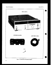
Mudcl 8671A and Accessories Supplied
Special Interconnect Cable
Line Voltage and Fuse Selection
Power Cable and Mains Plug Part Numbers
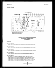
Locatiorl OK IIY.IB Address and
Parallel Poll Switches, .
Hewlett-Packard Interface Bus Connection
Front Panel Connectors, Controls; Switches
and Displays
Rear Panel Controls, Connectors, and
Indicators
Operator’s Frequency and Modulation
Checks Test Setup
r‘xequency Prugramming
Typical Freqoency Switching Time for the
8671A Synthesizer Showing Worst Case
Lock and Settling Times
Programming Examples
10 MHz Reference Oscillator Adjustment
‘hst Setup.
VCXO Adjustment Test Setup
M/N Loop Adjustment Test Setup
YTO Loop Sampler Adjustment
Test Setup.
Typical Swept Frequency Response at
A3A9A5TPl (Frequency span per
division 20 MI-Ii;)
YTO Loop Of&t and FM Overmodulation
Adjustment Test Setup
YTO Loop Offset Adjustment Waveforms
YTO Loop Phase Detector Adjustment
‘Test Selup
Spectrum Analyzer Display of Phase-Locked
LoopGain......................
0/I Driver Adjustment Tebt Setup
5.5
5.8
5"ll
8.24.
3.25.
3.26.
A3A9 Assembly in Service Position R-10
Qualifiers S-11,
Contiguous Blocks 8-11
Indicator Symbols S-12
AND Dependency Notation 8”13
OR and Free Dependency Notation 8.13
AND Dependency Notation, Coder Example
using Letters 8.13
Common Control Block 8.14
Quad D-Type Latch (Individual) 8.14
Quad D-Type Latch (Combined) S-14
Quad D.Type Latch Example S-14
Multiplexer (AND.OR Selected) Example S-15
Shift Register Example 8-15
Up.Down Counter Example 8-15
Synthesizer’s Simplified Block Diagram 8-24
Major Afisembly Locations 8.24
Overall Troubleshooting Block Diagram 8-29
A3 RF Source Assembly Troubleshooting
Block Diagram 8-33
A2 Controller Assembly Troubleshooting
Rlock Diagram 8.35
Al RF Output Assembly Block Diagram 8.37
AlAl Front Panel Assembly Component,
Adjustment, and Test Point Locations 8.31
AlAl Front Panel Assembly
5.13 8-21.
5.14
5.15
5-16
8.28.
8.29.
8-30.
8-31.
8-32.
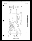
Schematic Diagram 8.37
A2A5 ZOj30 MHz Divider Assembly
Component, Adjustment and Test Point
Location 8-38
20130 MHz Divider ‘Block Diagrams 8-39
20/30 MHz Divider Assembly
Schematic Diagram 8-39
A2A4 20/30 MHz Phasp Detector Assembly
Component, Adjustment, and Test Point
Locations 8-40
ZOj30 MHz Phase Detector Block Diagrams 8.41
20130 MHz Phase Detector Assembly
Schematic Diagram S-41
Typical Output Power from 8671A
SWR Test Setup
FM Accurtxy Test Setup
Power Line Related Spurious Test Setup
Signal-to-Phaw Noise Retiu Test Setup
FM Frequency Response ‘Test Setup
FM Dietortiorl Test Setup
Residual FM in FM and CW Modes
Test Setup.
Frequency Switching Time Test Setup
Internal Time Base Aging Rate
Test Setup.
2.1
2-2
2.4
2-5
3-2
3.3
3-5
'3.10
3"12
3.14
4-2
4.5
4.7
4-9
'4-u
4.13
4.15
4.18
4-21
4.24
FIgwe
Page
5.11.
5.12.
5-18.
6”l.
6-2.
6.3.
8.1.
8.2.
8-3.
8.4.
3"5.
3.6.
8.7.
8.8.
8-9.
S-10.
8.11.
8.12.
8.13.
8.14.
S-15.
S-16.
8.17.
S-18.
E-19.
8.20.
8-21.
E-22.
8.23.
20130 MHz Loop Divider Bias Adjustment
Test Setup. 5.22
A2A4 Assembly Notch Filter Adjustment
Test Setup.
5.23
FM Sensitivity Adjustment Test Setup 5.24
Al Assembly, Front Panel Mechanical Parts 6.6
A2 Assembly, Front Panel Mechanical Parts. 6-20
Synthesizer Chassis Parts 6.41
Schematic Diagram Notes 8-2
Rear Panel of the Synthesizer 8-7
A2 Assembly Front Panel Fully Extended 8.8
httom of the Synthesizer 8-9