


Model 8671A
contents
ILLUSTRATIONS (Cont’d)
Figure Page
8.33.
8.43.
8~35.
H-36.
8.37.
8-38.
H-39.
8.40.
8-11.
&i”42.
M-43.
8.44.
H”45.
H-16.
8.47.
H-48.
H-51.
8-54.
8.55.
M”5ti.
8.57.
8-58.
8.59.
MO.
8-61.
8.82.
8.63.
8.64.
8-65.
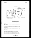
A2A3 160-240 MHz Assembly Component
Locations R-42
VCO 160-240 MHz Lllock Diagrams 8-43
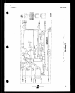
VCO ‘160-240 MHz Assembly Schematic
Diagram 8-48
KM9 HP-IB Addresfi Assembly Cumponent
Localiuns 8.44
HP-It< Address Block Diagrams 8.45
HP-ID Address Assembly Schematic Diagram 8-45
P/O h2h7 Interface Assembly Component
and Tesl Point Locations 8.46
P/O Jntexfnce Block Dia@ams 8.47
P/O HP-Ii3 Interface Assembly Schematic
Diagram 8-47
P/O A2Al interface Assembly Component
Locations 8.48
P/O lntsrface Block Diagrams 8.49
P/O Interface Assembly Schematic Diagram 8-49
A2A10 Register 1 Assembly Component
Locations 8-50
Register 1 block Diagrams 8-51
Register 1 Assembly Schematic Diagram 8-51
P/O A2All Timing and Control Assembly
Componenl and Test Point Locations 8-52
P/O Timing and Control Block Diagrams 8-53
P/O Timing and Corltrul Assembly Schematic
Diagram 8-53
U/O A2All Timing and Control Assembly
Component and
Test
Point Localiuns 8-54
U/O Timing and Control Block Diagrams R-55
P/D Timing and Control Assembly Schematic
Diagram 8.55
P/O A2A8 Output Register Assembly
Component and ‘Test Point Locations 8-56
P/O Ch~lpul Register Klock Diagrams 8.57
P/O Output Register Assembly Schematic
Diagram 8-57
V/O h2AM Output llegister Assembly
Cumpununt and Test Point Locations 8.58
P/O Output Kegister Block Diagrams 8.59
P/O Oolpul Register Assrmhly Schematic
Diagram 8-59
I’/0 A2Al Krront Panel Assembly Component
Lucations 8.60
P/O Front Parwl Block Diagrams 8.61
P/O Front Panel Assembly Schematic
Diagram 8.61
P/O A2Al Front Panel Assembly
Component Locatiorrs 8.62
P/O Pront Panel Block Diagrams 8.63
P/O Front Panel Assembly Schfmatic
DiaKram 8-63
8-66.
8-67.
8”68.
8-69.
8.70.
8-71.
8.72,
s-73.
8.74.
8-75.
8.76.
8-77.
8.78.
8.79.
8.80.
8.81.
8.82.
S-83.
8.84.
8.85.
8.86.
8.87.
8.88.
S-89.
S-90.
8-91.
8.92.
R-93.
8.94.
8.95.
A3AlAl Reference J’hase Lock Board
Assembly Component and Test Point
Locations 8-64
Hefexsnce Phase Lock Block Diagrams 8.65
Refcrencc Phase Lock Assembly Schematic
Diagram 8-65
A3AlA2 100 MHz VCXO Assembly
Component, Adjustment, and Test
Point Locations 8-66
100 MHz VCXO Block iliagxams 8-67
100 MHz VCXO Assembly Schematic
Diagram 8-81
A3AlA3 M/N Phase Detector Assembly
Component and Test Point Locations 8-68
M/N Phase Deteclur Block Diagrams. 8.69
M/N Phase Detector Assembly Schematic
wiagxam 8.69
A3AlA4A2 M/N VCO Board Assembly
Component, Adjustment, and Test Point
Locations 8.70
M/N VCO Rlock Diagrams. 8-71
M/N VCO Assembly Schematic Diagram 8-71
A3AlA5 M/N Output Assembly Component
Locations 8-72
M/N Output Block Diagrams. 8-78
M/N Output Assembly Schematic Diagram 8-73
A3A5 DAC Asscmhly Component,
Adjustment, and Test Point Locations H-14
Wigital-Lo-Analog Converter Block
Diagrams. 8-75
Digital.to.Analog Converter Schematic
Diagram 8”75
A3A6 YTO Main Coil Driver Assembly
Component, Adjustment, and Test Point
Localions 8-76
YTO Main Coil Driver Block Diagrams 8.77
YTO Main Coil Driver Schematic Diagram 8.77
A3A9A5 YTO Sampler Assembly Component
Adjustment, and Test Point Locations R-78
YTO Sampler Block Diagrams 8.79
YTO Sampler Assembly Schematic
nisgram 8.79
ABAYA4 YTO Phase Detector Assembly
Component, Adjustment, and Test Point
Locations ; sao
YTO Phase Detector Block Diagrams R-81,
YTO Phase Detector Assembly Schematic
Diagram 8-81
A3A7 FM Driver Assembly Component,
Adjustment, and Test Point Locations 8-82
FM Driver Block Diagrams 8.83
FM Driver Assembly Schematic Diagram 8.83