


HUAWEI ME909 Series Mini PCIe Module
Hardware Guide
Description of the Application Interfaces
Issue 0.1 (2013-06-09)
Huawei Proprietary and Confidential
Copyright © Huawei Technologies Co., Ltd.
14
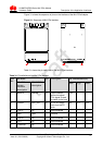
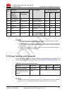
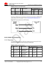
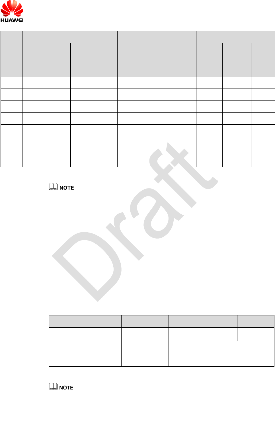
PIN
No.
Pin Name
I/O
Description
DC Characteristics (V)
Mini PCI
Express
Standard
Description
HUAWEI Pin
Description
Min.
Typ.
Max.
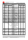
46
LED_WPAN#
NC
-
Not connected
-
-
-
47
Reserved
PCM_DOUT
O
PCM I/F data out
–0.3
1.8
2.1
48
1.5 V
NC
-
Not connected
-
-
-
49
Reserved
PCM_DIN
I
PCM I/F data in
–0.3
1.8
2.1
50
GND
GND
-
Ground
-
-
-
51
Reserved
PCM_SYNC
O
PCM interface sync
–0.3
1.8
2.1
52
3.3Vaux
VCC_3V3
P
3.3 V DC supply rail
from the PC side.
3.0
3.3
3.6
P indicates power pins; I indicates pins for digital signal input; O indicates pins for digital
signal output. AI indicates pins for analog signal input.
The Reserved pins are internally connected to the module. Therefore, these pins should not
be used, otherwise they may cause problems. Please contact with us for more details about
this information.
The NC (Not Connected) pins are floating and there are no signal connected to these pins.
Therefore, these pins should not be used.
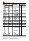
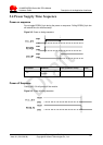
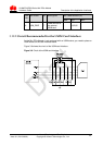
3.3 Power Sources and Grounds
For the Mini PCIe Adapter, +3.3 Vaux is the only voltage supply that is available. The
input voltage is 3.3 V±9%, as specified by PCI Express Mini CEM Specifications 1.2.
Table 3-2 Power and ground specifications
Pin No.
Pin Name
Minimum
Typical
Maximum
2, 24, 39, 41 and 52
VCC_3V3
3.0 V
3.3 V
3.6 V
4, 9, 15, 18, 21, 26, 27,
29, 34, 35, 37, 40, 43,
and 50
GND
-
To minimize the RF radiation through the power lines, it is suggested to add ceramic capacitors
of 10 pF and 100 nF in the power lines beside the Mini PCIe connector on the host side.