


— 6 —
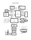
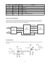
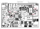
CPU (LSI105: UPD912GF-3BA)
The 16-bit CPU contains a 1k-byte RAM, three 8-bit I/O ports, two timers, a keycontroller and serial interfaces.
The CPU detects key velocity by counting the time between first-key input signal FI and second-key SI from
the keyboard. The CPU reads sound data and velocity data from the sound source ROM in accordance with
the selected tone; the CPU can read rhythm data simultaneously when a rhythm pattern is selected. Then the
CPU provides 16-bit serial sound data to the DSP. The CPU also controls MIDI input/output and stores
sequencer data into the working storage RAM.
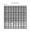
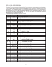
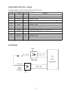
The following table shows the pin functions of LSI105.
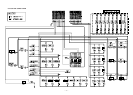
Pin No. Terminal In/Out Function
1 TXD0 Out MIDI signal input
2 RXD0 In MIDI signal output
3 SCK0 Out APO (Auto Power Off) signal output
4, 5 TXD1, RXD2 — Not used. Connected to ground.
6 SCK1 Out 1 MHZ synchronizing pulse output
7 AVCC In Ground (0 V) source
8, 9 AN0, AN1 — Not used. Connected to ground.
10 AGND In Ground (0 V) source
11 BCK Out Bit clock output
12 SO Out Serial sound data output
13 LRCK Out Word clock output
14 GND In Ground (0 V) source
15, 16 XLT0, XLT1 In/Out 20 MHz clock input/output
17 VCC In +5 V source
18, 19 MD0, MD1 In Mode selection terminal
20 RSTB In Reset signal input
21 NMI In Power ON signal input
22 INT — Not used. Connected to ground.
23 ~ 30
FI0 ~ FI3
SI0 ~ SI3
In Terminal for key input signal
31 ~ 38 KC0 ~ KC7 Out Terminal for key scan signal
39 ~ 46
FI4 ~ FI7
SI4 ~ SI7
In Terminal for key input signal
47, 48 FI8, SI8 In Terminal for pad input signal
49 FI9 In Terminal for button input signal
50 SI9 In Sustain signal input
51 FI10 In Terminal for button input signal
52 SI10 In Not used
53 ~ 55 KI0 ~ KI2 In Terminal for button input signal
56 MWNB Out Write enable signal output
57 ~ 76 MA0 ~ MA17 Out Address bus
77 MCSB0 Out Chip enable signal output for the sound source ROM
78 MCSB1 Out Not used
79 MCSB2 Out Chip enable signal output for the DSP