


— 9 —
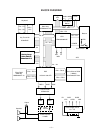
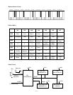
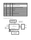
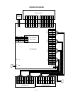
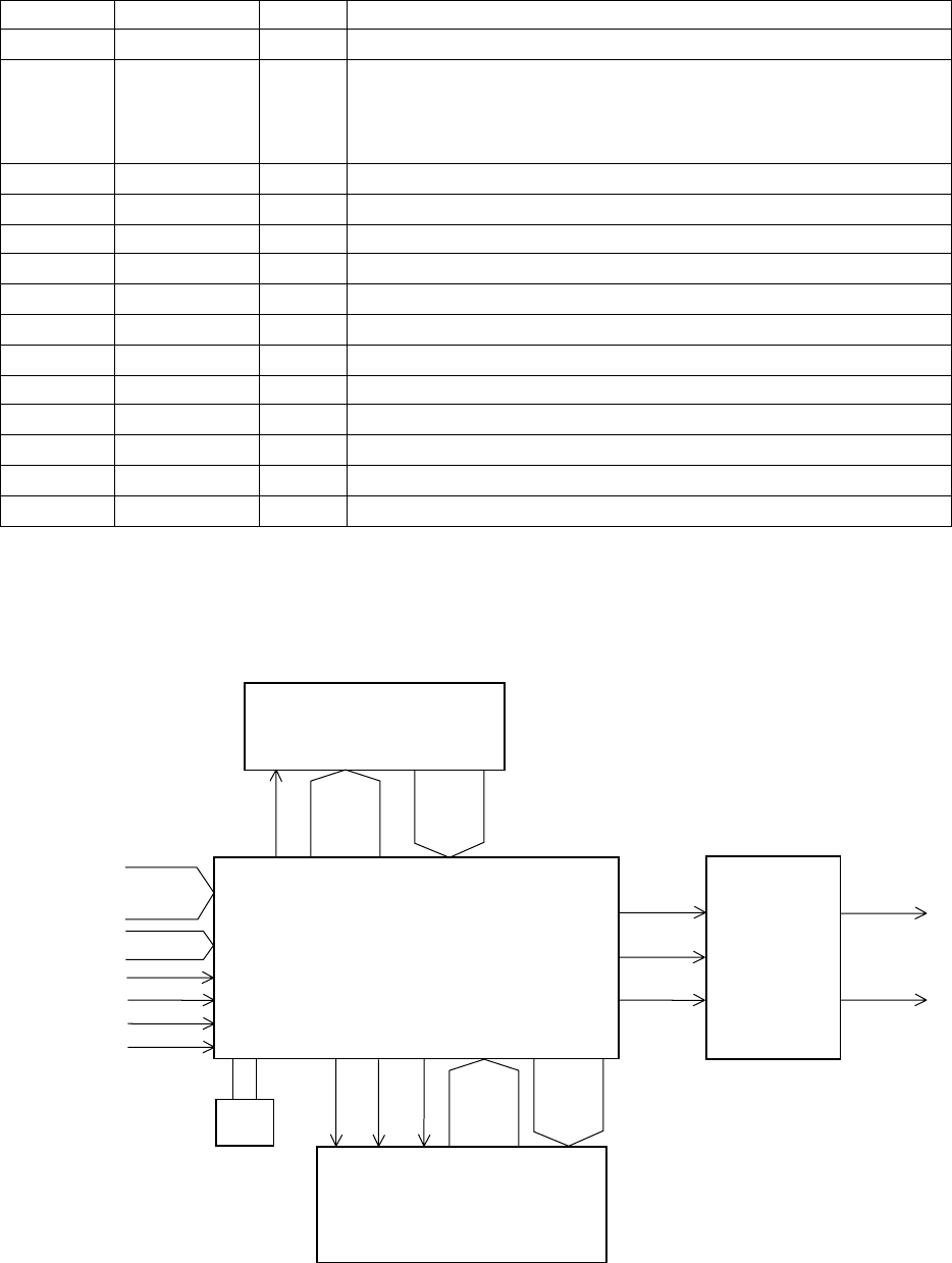
DSP
HG51A115A01FD
Effect RAM (256K-bit)
HM65256BLP
Sound Source ROM
TC5316200CP-C081
CE
A0 ~ A19 D0 ~ D15
RA0 ~
RA19
RD0 ~
RD15
RA22
D0 ~ D7
A0 ~ A3
LSIS
RDAPO
WRAPO
RESET
SOLP
BOK
WOK1
EA0 ~
EA14
ED0 ~
ED15
CS
WE
OE
D0 ~ D15
A0 ~ A14
ECEB EOEB
EWEB
PG
16.384MHz
DAC
UPD6376CX
LOUT
ROUT
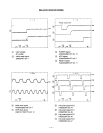
SOLP: Sound data
BOK: Bit clock
WOK1: Word clock
SI
CLK
LRCK
Block diagram of DSP and DAC circuit
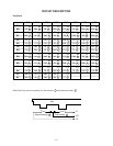
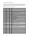
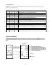
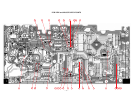
Pin No. Terminal In/Out Function
93 VCC5 In +5V source
94, 95
97 ~ 105
107,109
110, 112
EA0 ~ EA14 Out Address bus for the effect RAM
96 EWEB Out Write enable signal output for the effect RAM
106 EOEB Out Read enable signal output for the effect RAM
108 VCC7 In +5V source
111 ECEB Out Chip select signal output for the effect RAM
113 ~ 117 Not used.
118 VCC4 In +5V source
119 GND4 In Ground (0V) source
120 ~ 122 Not sued.
123 ~ 130 ED0 ~ ED7 In/Out Data bus for the effect RAM
131 GND5 In Ground (0V) source
132 ~ 134 Not used. Connected to ground.
135, 136 Not used.