


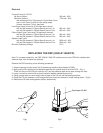
— 7 —
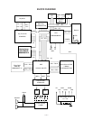
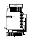
Gate Array (UPD65005C-578)
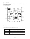
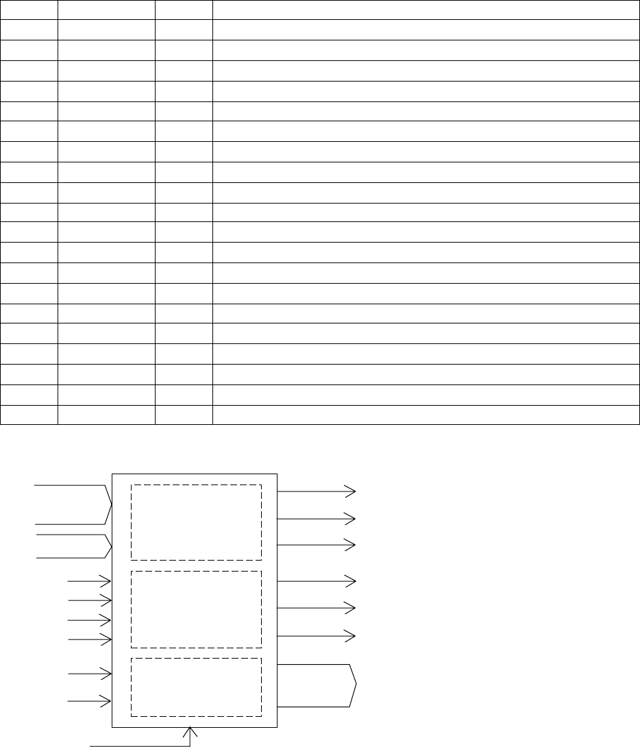
Functions of the gate array are;
(1) To decode chip select signals for the working strage RAM, the DSP and the key touch LSI.
(2) To hold the following signals on "Low" during power off.
Read/write enable signals for the DSP and the key touch LSI
10MHz clock for the key touch LSI
(3) To generate button scan / LED drive signals.
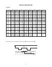
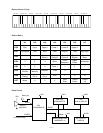
The following table shows the pin functions of the gate array.
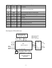
A4 ~ A15
D0, D1
RD
WR
PHA
APO
KOD
KOC
RESET
LSIS
HG
SRAM
RDAPO
WRAPO
PHAPO
KO0 ~ KO7
Address decoder
Controller
Shift register
(Chip select sigal for the DSP)
(Chip select signal for the key touch LSI)
(Chip select signal for the working strage RAM)
(Read enable signal controlled by APO)
(Write enable signal controlled by APO)
(10MHz clock for the key touchLSI.
Controlled by APO)
(Button scan / LED drive signal)
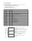
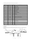
Pin No. Terminal In/Out Function
1 -RESET In Reset signal input
2 -RDAPO Out Read enable signal output
3 -WRAPO Out Write enable signal output
4 -LSIS Out Chip select signal for the DSP
5 -HG Out Chip select signal for the key touch LSI
6 PHAPO Out 10MHz clock for the key touch LSI
7 -SRAM Out Chip select signal for the working strage RAM
8 ~ 9 KO8 ~ KO9 Not used.
10 ~ 17 KO7 ~ KO0 Out Button scan / LED drive signal output
18 ~ 20 Not used.
21 GND In Ground (0V) source
22 PHA In 10MHz clock input
23 -WR In Write enable signal input
24 -RD In Read enable signal input
25 -APO In APO (Auto Power Off) signal input
26 KOC In KO signal data input
27 KOD In Clock for KO signal data
28 ~ 39 A15 ~ A4 In Address bus
40, 41 D0, D1 In Data bus
42 VDD In +5V source