


— 15 —
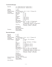
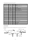
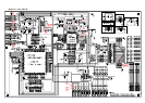
AVDD
1K
1K 1K
C222(H)
C103(H)
AG
AG
1K
AG
To main volume
-
+
IC105
M5218APR
10V22µ
C333(H)
Q107/108
2SC1740
18K
50V1µ
From the DAC
1K
AG
AVDD
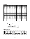
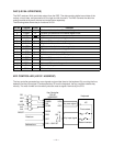
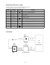
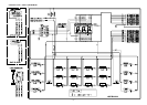
The following table shows the pin functions of LSI107.
Pin No. Terminal In/Out Function
1 REQB Out Not used
2, 3, 60 ~ 63
FI8 ~ FI10,
SI8 ~ SI10
In Not used. Connected to + 5V.
4 VCC In +5V source
5 CRDB In Read enable signal input
6 CWRB In Write enable signal input
7 CCBB In Chip select signal input
8, 9, 11 T, STBY, W In Not used. Connected to +5V.
10 RESB In Reset signal input
12 CKI In 10 MHz clock input
13, 14 TMD, TST In Not used. Connected to ground.
15 CKO Out Not used.
16 GND In Ground (0V) source
17 XIN In Not used. Connected to ground.
18 XOUT Out Not used.
19 TRES In Not used. Connected to ground.
20 ~ 23, 25 ~ 28 CD0 ~ CD7 In/Out Data bus
24 GND In Ground (0V) source
29 ~ 31 CR0 ~ CR2 In Address bus
32 VCC In +5V source
33 ~ 39, 41 ~ 43
53 ~ 55, 57 ~ 59
FI0 ~ FI7,
SI0 ~ SI7
In Key input signal input
40 VCC In +5V source
44 ~ 47, 49 ~ 52 KC0 ~ KC7 Out Key scan signal
48, 56 GND In Ground (0V) source
64 VCC In +5V source
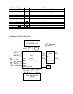
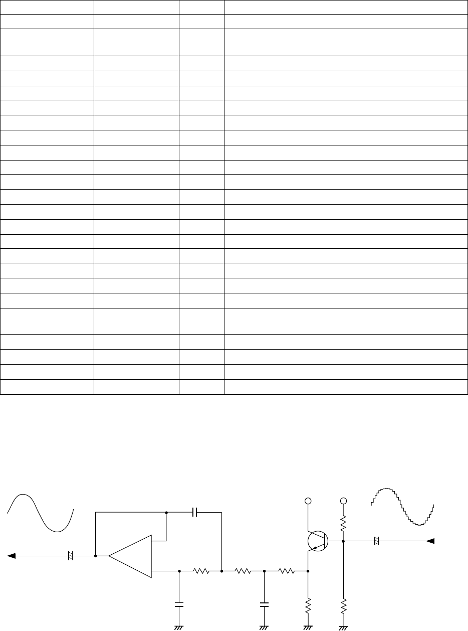
FILTER BLOCK
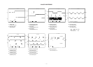
Since the sound signals from the DAC are stepped waveforms, the filter block is added to smooth the
waveforms.