


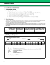

MB15F74UL
12
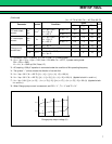
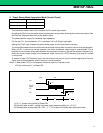
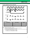
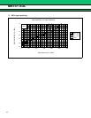
4. Serial Data Data Input Timing
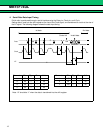
Divide ratio is performed through a serial interface using the Data pin, Clock pin, and LE pin.
Setting data is read into the shift register at the rise of the Clock signal, and transferred to a latch at the rise of
the LE signal. The following diagram shows the data input timing.
LSBMSB
Clock
Data
LE
t7
t1 t2 t3
t4 t5
t6
1st data 2nd data
Control bit
Invalid data
Note : LE should be “L” when the data is transferred into the shift register.
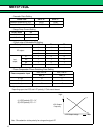
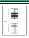
Parameter Min Typ Max Unit Parameter Min Typ Max Unit
t
1 20 ns t5 100 ns
t
2 20 ns t6 20 ns
t
3 30 ns t7 100 ns
t
4 30 ns