


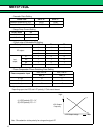

MB15F74UL
3
■
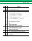
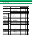
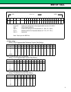
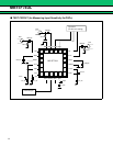
PIN DESCRIPTION
Pin no.
Pin
name
I/O Descriptions
1fin
IF I
Prescaler input pin for the IF-PLL.
Connection to an external VCO should be AC coupling.
2Xfin
IF I
Prescaler complimentary input for the IF-PLL section.
This pin should be grounded via a capacitor.
3GND
IF Ground pin for the IF-PLL section.
4VCCIF
Power supply voltage input pin for the IF-PLL section (except for the charge pump
circuit) , the shift register and the oscillator input buffer.
5PS
IF I
Power saving mode control pin for the IF-PLL section. This pin must be set at “L” when
the power supply is started up. (Open is prohibited.)
PS
IF = “H” ; Normal mode/PSIF = “L” ; Power saving mode
6Vp
IF Power supply voltage input pin for the IF-PLL charge pump.
7DoIF O Charge pump output for the IF-PLL section.
8 LD/fout O
Lock detect signal output (LD) /phase comparator monitoring output (fout) pin. The
output signal is selected by LDS bit in a serial data.
LDS bit = “H” ; outputs fout signal/LDS bit = “L” ; outputs LD signal
9Do
RF O Charge pump output for the RF-PLL section.
10 VpRF Power supply voltage input pin for the RF-PLL charge pump.
11 PS
RF I
Power saving mode control for the RF-PLL section. This pin must be set at “L” when the
power supply is started up. (Open is prohibited. )
PS
RF = “H” ; Normal mode/PSRF = “L” ; Power saving mode
12 V
CCRF
Power supply voltage input pin for the RF-PLL section (except for the charge pump
circuit)
13 GND
RF Ground pin for the RF-PLL section
14 XfinRF I
Prescaler complimentary input pin for the RF-PLL section.
This pin should be grounded via a capacitor.
15 fin
RF I
Prescaler input pin for the RF-PLL.
Connection to an external VCO should be via AC coupling.
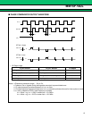
16 LE I
Load enable signal input pin (with the schmitt trigger circuit)
When LE is set “H”, data in the shift register is transferred to the corresponding latch
according to the control bit in a serial data.
17 Data I
Serial data input pin (with the schmitt trigger circuit)
Data is transferred to the corresponding latch (IF-ref. counter, IF-prog. counter, RF-ref.
counter, RF-prog. counter) according to the control bit in a serial data.
18 Clock I
Clock input pin for the 23-bit shift register (with the schmitt trigger circuit)
One bit data is shifted into the shift register on a rising edge of the clock.
19 OSC
IN I
The programmable reference divider input pin. TCXO should be connected with an AC
coupling capacitor.
20 GND Ground pin for OSC input buffer and the shift register circuit.