


Philips Semiconductors Product specification
SA70161.3GHz low voltage fractional-N synthesizer
1999 Nov 04
11
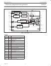
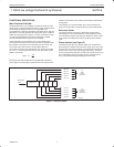
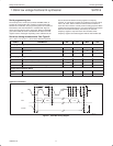
Serial programming bus
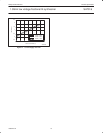
The serial input is a 3-wire input (CLOCK, STROBE, DATA) to
program all counter divide ratios, fractional compensation DAC,
selection and enable bits. The programming data is structured into
24 bit words; each word includes 2 or 3 address bits. Figure 8
shows the timing diagram of the serial input. When the STROBE
goes active HIGH, the clock is disabled and the data in the shift
register remains unchanged. Depending on the address bits, the
data is latched into different working registers or temporary
registers. In order to fully program the synthesizer, 3 words must be
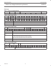
sent: C, B, and A. Table 1 shows the format and the contents of
each word. The D word is normally used for testing purposes. When
sending the B-word, data bits FC7–0 for the fractional compensation
DAC are not loaded immediately. Instead they are stored in
temporary registers. Only when the A-word is loaded, these
temporary registers are loaded together with the main divider ratio.
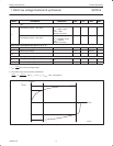
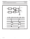
Serial bus timing characteristics. See Figure 8.
V
DD
= V
DDCP
=+3.0V; T
amb
= +25°C unless otherwise specified.
SYMBOL
PARAMETER MIN. TYP. MAX. UNIT
Serial programming clock; CLK
t
r
Input rise time – 10 40 ns
t
f
Input fall time – 10 40 ns
T
cy
Clock period 100 – – ns
Enable programming; STROBE
t
START
Delay to rising clock edge 40 – – ns
t
W
Minimum inactive pulse width 1/f
COMP
– – ns
t
SU;E
Enable set-up time to next clock edge 20 – – ns
Register serial input data; DATA
t
SU;DAT
Input data to clock set-up time 20 – – ns
t
HD;DAT
Input data to clock hold time 20 – – ns
Application information
SR01417
CLK
DATA
STROBE
ADDRESS LSB
t
SU;DAT
t
HD;DAT
t
r
t
w
t
f
t
SU;E
t
START
T
cy
MSB
Figure 8. Serial Bus Timing Diagram