


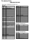
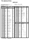
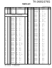

TK-260G/270G
18
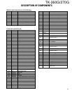
CIRCUIT DESCRIPTION
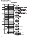
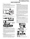
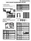
Fig. 4 AF Amplifier and Squelch
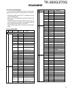
Fig. 5 PLL circuit
5) Audio amplifier circuit
The demodulated signal from IC4 is amplified by IC16 (2/
2), high-pass filtered, low-pass filtered, high-pass filtered,
band-eliminate filtered, and de-emphasized by IC14.
The signal then goes through an AF amplifier IC15 (2/2),
an AF volume control (VR2), and is routed to an audio
power amplifier (IC11) where it is amplified and output to
the speaker.
6) Squelch
Part of the AF signal from the IC enters the FM IC (IC4)
again, and the noise component is amplified and rectified
by a filter and an amplifier to produce a DC voltage
corresponding to the noise level.
The DC signal from the FM IC goes to the analog port of
the microprocessor (IC13). IC13 determines whether to
output sounds from the speaker by checking whether the
input voltage is higher or lower than the preset value.
To output sounds from the speaker, IC6 sends a high signal
to the SP MUTE line and turns IC11 on through
Q32,Q33,Q34 and Q30.(See Fig. 4)
7) Receive signaling
(1) QT/DQT (Low-speed data)
300Hz and higher audio frequencies of the output signal
from IF IC are cut by a low-pass filter (IC19). The resulting
signal enters the microprocessor (IC13). IC13 determines
whether the QT or DQT matches the preset value, and
controls the SP MUTE and the speaker output sounds
according to the squelch results.
(2) 2-TONE (High-speed data)
Part of the received AF signal output from the AF amplifier
IC16(2/2), and then passes through an audio processor
(IC14), goes to the other AF amplifier IC15(1/2), is
compared, and ther goes to IC13. IC13 checks whether 2-
TONE data is necessary. If it matches, IC13 carries out a
specified operation, such as turning the speaker on. (See
Fig. 4)
DET
IC13
CPU
IF AMP
IC16 (2/2)
IF AMP
IC19
LPF
QT/DQT
2TN
2-TONE
IC15 (1/2)
COMPARATER
IC18
DTMF
DECODE
PD, CLK, SD,STD
93ANSQL
TOI
95
FM IF IC4
5
43
Q36
SW
Q32, 33, 34
SW
DE-
EMP
MUTE
EXP
HPF LPF HPF BEF
IC14
21
IC15 (2/2)
AF AMP
41
IC11
AF PA AMP
Q30
SW
SP
OUTPUT
EXPANDER
IC6
5RC
SP
MUTE
5
7
3
PLL DATA
16.8MHz
REF OSC
I/M
I/N
PLL IC IC2
PHASE
COMPARATOR
CHARGE
PUMP
LPF
5kHz/6.25kHz
D2, 4
D9, 11
Q2
TX VCO
Q10
RX VCO
Q3
BUFF AMP
Q4
RF AMP
Q1
RF AMP
Q7, 8
T/R SW
5kHz/6.25kHz
(3) DTMF (High-speed data)
The DTMF input signal from the IF IC(IC4) is amplified by
IC16(2/2) and goes to IC18, the DTMF decoder. The decoded
information is then processed by the CPU. During
transmission and standby, the DTMF IC is set to the power
down mode when the PD terminal is High. When the line is
busy, the PD terminal becomes Low, the power down mode
is canceled and decoding is carried out.
3. PLL frequency synthesizer
The PLL circuit generates the first local oscillator signal for
reception and the RF signal for transmission.
1) PLL
The frequency step of the PLL circuit is 5 or 6.25kHz.
A 16.8MHz reference oscillator signal is divided at IC2 by a
fixed counter to produce an oscillator (VCO) output signal which
is buffer amplified by Q3 then divided in IC2 by a dual-module
programmable counter. The divided signal is compared in
phase with the 5 or 6.25kHz reference signal from the phase
comparator in IC2. The output signal from the phase
comparator is filtered through a low-pass filter and passed to
the VCO to control the oscillator frequency.(See Fig. 5)
2) VCO
The operating frequency is generated by Q2 in transmit
mode and Q10 in receive mode. The oscillator frequency is
controlled by applying the VCO control voltage, obtained from
the phase comparator, to the varactor diodes (D2 and D4 in
transmit mode and D9 and D11 in receive mode). The T/R pin
is set high in receive mode causing Q7 and Q8 to turn Q2 off
and Q10 on.
The T/R pin is set low in transmit mode. The outputs from
Q10 and Q2 are amplified by Q3 and sent to the buffer
amplifiers.
The outputs from Q3 to Q4 is divided into 1/2 in passing
through a Divider IC (IC301), and goes to the RF amplifiers.