


OMB-DAQ-2416-4AO User's Guide Specifications
41
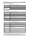
Analog input/output calibration
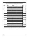
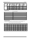
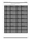
Table 24. Analog input/output calibration specifications
Parameter
Specifications
Recommended warm-up time
45 minutes minimum
Calibration
Firmware calibration
Calibration interval
1 year
Calibration reference
+10.000 V, ±5 mV maximum. Actual measured values stored in EEPROM
Tempco: 5 ppm/°C maximum
Long term stability: 30 ppm/1000 hours
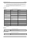
Digital input/output
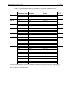
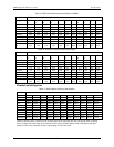
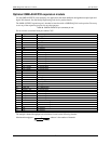
Table 25. Digital input specifications
Number of I/O
8 channels
Configuration
Each DIO bit can be independently read from (DIN) or written to (DOUT).
The DIN bits can be read at any time whether the DOUT is active or tri-stated.
Input voltage range
0 to +15 V
Input type
CMOS (Schmitt trigger)
Input characteristics
47 kΩ pull-up/pull-down resistor, 28 kΩ series resistor
Maximum input voltage range
0 to +20 V maximum (power on/off, relative to DGND pins 93 and 94)
Pull-up/pull-down
configuration
All pins pulled up to +5 V via individual 47 kΩ resistors (the JP1 shorting block
default position is pins 1 and 2).
Pull down capability is available by placing the JP1 shorting block across pins 2 and 3.
Transfer rate (software paced)
500 port reads or single bit reads per second typical.
Input high voltage
1.3 V minimum, 2.2 V maximum
Input low voltage
1.5 V maximum, 0.6 V minimum
Schmitt trigger hysteresis
0.4 V minimum, 1.2 V maximum
Note 2: DGND pins (pins 93, 94) are recommended for use with digital input and digital output pins. The
DGND and GND pins are common and are isolated from earth ground.
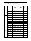
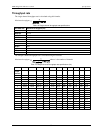
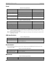
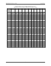
Table 26. Digital output specifications
Number of I/O
8 channels
Configuration
Each DIO bit can be independently read from (DIN) or written to (DOUT).
The DIN bits may be read at any time whether the DOUT is active or tri-stated
Output characteristics
47 kΩ pull-up, open drain (DMOS transistor)
Pull-up configuration
All pins pulled up to +5 V via individual 47 kΩ resistors (the JP1 shorting block
default position is pins 1 and 2).
Transfer rate (software paced)
Digital output – 500 port writes or single-bit writes per second typical.
Output voltage range
0 to +5 V (no external pull up resistor, internal 47 kΩ pull-up resistors connected to
+5 V by default)
0 to +15 V maximum (Note 5)
Drain to source breakdown
voltage
+50 V minimum
Off state leakage current
(Note 6)
0.1 µA
Sink current capability
150 mA maximum (continuous) per output pin
150 mA maximum (continuous) for all eight channels
DMOS transistor on-resistance
(drain to source)
4 Ω
Note 3: Each DMOS transistor’s source pin is internally connected to GND.
Note 4: DGND pins (pins 93, 94) are recommended for use with digital input and digital output pins. The
DGND and GND pins are common and are isolated from earth ground.