


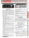
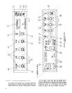
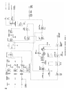
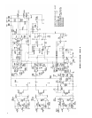
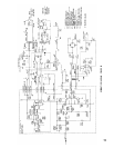
THEORY OF OPERATION (Cont’d)
maximum of 30 dB, the second potentiometer section acts
as a conventional voltage divider output attenuator for low
control settings. The input transformers increase the signal
voltage by 21 dB.
Input 1 has a second line input, phone jack J12, which
operates only in the LINE position of S9. Additionally, this
stage (Q109, 110, 111) may be converted to a level-stabil-
ized, low distortion, 1 kHz Wien bridge tone oscillator.
A feedback-type, virtual-ground, low gain (3 dB) mixing
amplifier (Q112, 113, 114) assures nearly zero interaction
among input level control settings. Each input to the mixing
stage has a resistance-capacitance low frequency rolloff
filter providing a 6 dB per octave slope, 3 dB down at about
150 Hz. The mix bus jack (J5) contains a switch so that
when a phono plug is inserted, the mix bus impedance is
increased from near zero to 3.9 K ohms, for compatibility
with conventional mixing systems.
Automatic gain reduction is accomplished by the voltage
variable FET attenuator, R401 and Q401. With signal levels
below compression threshold, or when compression is dis-
abled, the FET gate-to-source voltage is sufficiently neg-
ative to prevent FET conduction. Increased signal levels,
however, are sensed and the dc control voltage is in-
creased until the FET drain-to-source resistance is reduced
enough to maintain a nearly constant signal voltage across
Q401.
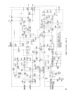
This compressed signal is applied to the Output Buffer
stage (Q402, 403, 404), which has variable feedback sim-
ilar to the input preamplifiers, via the dual-section Output
potentiometer. This assures optimum output-stage clipping
and noise characteristics, either with a constant, com-
pressed signal to the Output Buffer stage, or with com-
pression disabled. The output amplifier (Q508, 509, 510,
511) is a class -AB, fixed gain line driver stage transformer-
coupled to the output load. A tertiary winding on T4 pro-
vides a microphone level balanced output, and headphone
and unbalanced auxiliary outputs are also derived from
the output amplifier stage through appropriate pads.
A three-transistor circuit (Q504, 505, 506) provides
full-wave rectification and power amplification to drive the
meter (Ml) with proper damping characteristics for the
VU output level function. The gain of the VU driver circuit
is changed by S4 for the two VU ranges.
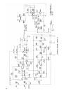
D.C. CONTROL GENERATION
The signal voltage appearing across the attenuator FET
(Q401) travels through a portion of the Output Buffer
(Q402, 403, 404) and a unity-gain Phase lnverter (Q405,
406, 407) to the Compression Buffer (Q408, 409), a 30-dB
gain stage. The output of this stage may be shorted to
ground by switch S14 to disable compression, or it may be
connected in parallel with a similar stage in a second SE30
via its Stereo Parallel jack (J8) so that stereo difference
signals will be canceled out and thus not compressed, and
the stereo sum will be the controlling signal.
The signal at this point enters a small class-B power
amplifier, the Rectifier Driver (Q501, 502, 503). A full-wave
diode bridge rectifier (D201, 202, 203, 204) is driven from
this amplifier through Driver Transformer T5, thus gen-
erating full-wave rectified, unfiltered pulses whose am-
plitude is proportional to the absolute value of the signal
across the attenuator FET (Q401).
The Response Rate control (R5) and capacitor C203
form a resistance-capacitance integration or averaging
network with an adjustable time constant so that a smooth
dc voltage is generated, equal to the average value of the
full-wave rectified pulses. This dc voltage is amplified
(X2) by the AC/DC Amplifier (MC201, Q105) and applied
to the gate of the attenuator FET (Q401). The AC/DC Am-
plifier has low input bias current to minimize its discharg-
ing effect upon the integrating capacitor (C203). An adjust-
ment associated with this amplifier applies an offset voltage
to the FET, setting the compression threshold.
The integrating R-C network assures an equal charge
and discharge time constant to provide a true average-
responding compression system. However, such a system
will exhibit a large overshoot in output when the input level
is suddenly increased. A Peak Detector (Q201, 203) is
therefore provided which monitors the instantaneous am-
plitude of the rectified pulses. If a pulse exceeds the av-
erage value by a preset amount, this detector will very
rapidly charge C203 enough to maintain the peak signal
amplitude within a reasonable upper limit. The Peak De-
tector threshold is set such that normal program material
at a constant level will not activate the circuit, but it will
reduce compressor gain rapidly for significant increases in
input level.
The AC/DC *Amplifier also has an input terminal for
signal voltage, fed via the Output Buffer and Phase In-
verter. This serves to apply one-half of the signal voltage
across FET Q401 to its gate, along with the dc control
voltage, thus reducing distortion due to the FET’s non-
linear resistance characteristic.
The dc control voltage applied to the gate of Q401 is
used to drive meter Ml through the dB Compression Meter
Amplifier (MC201, Q206). This amplifier has gain, offset, and
gain reduction adjustments to allow calibration of the
meter reading to correspond at three points to actual levels
of compression, despite the nonlinear relationship between
compression and dc control voltage.
GATED MEMORY
The Gated Memory Switch FET Q204 allows the in-
tegrating capacitor (C203) to be charged and discharged
as described under normal signal conditions. However,
when the input signal drops below compression threshold,
Q204 becomes an open circuit, preventing discharge of
C203 and maintaining the amount of gain reduction just
prior to the opening of the FET switch.
The Gated Memory Amplifier (MC301, Q306) receives
the uncompressed signal, proportional to input level, from
the Mixing Amplifier. A fast-acting voltage doubler rec-
tifier (D303, 304) converts this signal to a dc level which is
applied to the Comparator (MC301, Q304) after being
clamped by Q305 to assure fast recovery. The Comparator
output is a two-level dc signal applied to the gate of FET
Q204, and to the Gated Memory Indicator Driver (Q302,
303) to indicate the state of the Gated Memory circuit. The
gain of the Gated Memory Amplifier is adjustable to allow
setting the comparison threshold, and the switching FET
may be prevented from opening by switches S13 or S14.
When power is first applied to the SE30, approximately
30 seconds is required for the dc power supply voltages
to become properly established. During this interval, Timer
Q301 and Discharge Switch Q202 partially discharge inte-
grating capacitor C203, preventing a possible “latch-up”
condition due to a turn-on transient combined with Gated
Memory Switch Q204 being open.
11