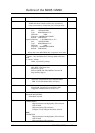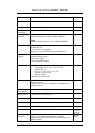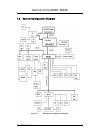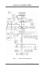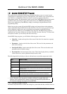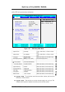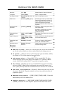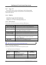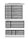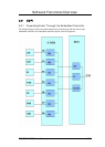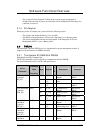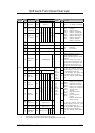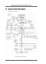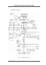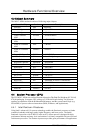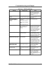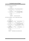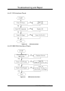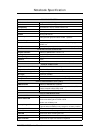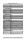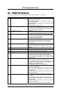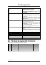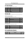
Software Functional Overview
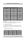
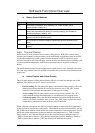
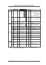
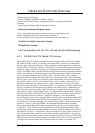
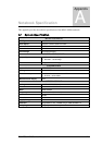
Register Bit Number
Function Address
Name
R/W
7 6 5 4 3 2 1 0
Logic
De-
fault
Description
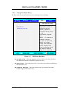
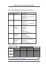
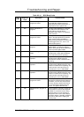
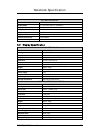
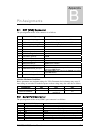
C0h
GPIO-C_
EVT_POL
R/W 0 0 0 0 0
0
POL_
C
[1:0]
0:
Falling
edge
1:
Rising
edge
0x00
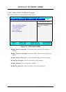
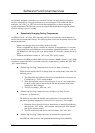
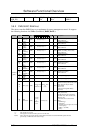
C1h
GPIO-C_
WAKE_ENB
R/W 0 0 0 0 0 0
WAK
E_
ENB
_C
[1:0]
0:
Disable
1:
Enable
0x00
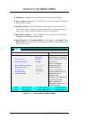
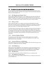
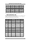
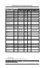
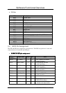
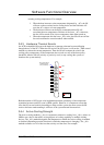
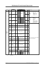
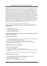
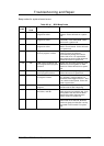
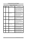
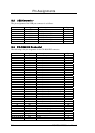
C2h EVT_CONT R/W
RES
[7:6]
W
A
K
E
S
C
I
R
E
S
*4
Q
_
R
U
N
W
A
K
E
_
O
U
T
S
U
S
_
X
0x00
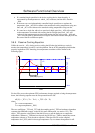
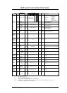
WAKE
SCI
Q_RU
N
WAKE
_OUT
SUS_X
=0: Wake# output is “Level”.
=1: Wake# output is “Pulse”.
=0: SCI is always output by
event detection and SCI_EVT
shows the query data is
stored. And next SCI is not
output until SCI_EVT is
cleared.
=1: SCI is output when the
command set is not executed
and OBF=0. SCI_EVT shows
the output SCI is for event
notification.
=0: Runtime event ststus is
reflected to RUN_EVT_STS
register.
=1: Runtime event status is
reflected to Query data.
=0: Wake event output is
always enable.( in S0-S3)
=1: Wake event output is
enable when SUS_X=L.
=0: Runtime and Wakeup is
selected by SUS_B.
(GPIO B6 is enable)
=1: Runtime and Wakeup is
selected by SUS_A.
(GPIO B6 is used as SUS_A
input.)
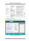
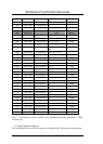
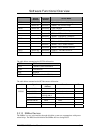
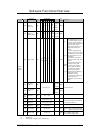
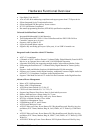
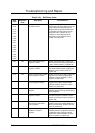
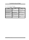
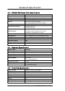
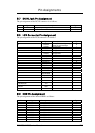
C3h
EC_RUN_
ENB_2
R/W
0:
Disable
1:
Enable
0x00
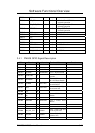
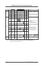
C4h
EC_WAKE_
ENB_2
R/W
Reserved [7:1]
T
H
0:
Disable
1:
Enable
0x00
TH: Thermal event
C5h
To
C7h
Reserved R/W
Don’t care
- -
C8h
*6
GPI_AD0 R AD0_DATA [7:0] - -
C9h
*6
GPI_AD1 R AD1_DATA [7:0] - -
For detail information, refer to GPIO
section in this document.
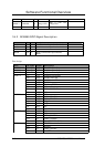
CAh
*6
Reserved R/W Don’t care - -
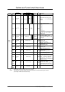
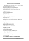
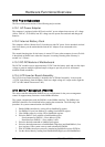
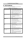
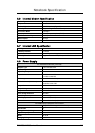
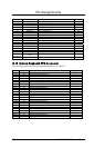
CBh D/A_CONT R/W DATA [7:0] - 0xff
0x00-0xfe: D/A converter output data
0xff : Battery capacity(%) output
Event/
GPIO
Control
CCh WAKE_DIS R/W DATA [7:0] - 0x00
0x00 : WAKE# output enable
0x01 : WAKE# output disable
*4: Should be 0.
*6: This register’s response time is 150usec max.
FIC M295 / M296 Service Manual 3-41