


General PowerPAD Design Considerations
1-17
General
1.12 General PowerPAD Design Considerations
The THS4012DGN IC is mounted in a special package incorporating a thermal
pad that transfers heat from the IC die directly to the PCB. The PowerPAD
package is constructed using a downset leadframe. The die is mounted on the
leadframe but is electrically isolated from it. The bottom surface of the lead
frame is exposed as a metal thermal pad on the underside of the package and
makes physical contact with the PCB. Because this thermal pad is in direct
physical contact with both the die and the PCB, excellent thermal performance
can be achieved by providing a good thermal path away from the thermal pad
mounting point on the PCB.
Although there are many ways to properly heatsink this device, the following
steps illustrate the recommended approach as used on the THS4012 EVM.
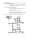
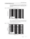
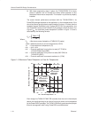
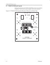
1) Prepare the PCB with a top side etch pattern as shown in Figure 1–8.
There should be etch for the leads as well as etch for the thermal pad.
Figure 1–8. PowerPAD PCB Etch and Via Pattern
Thermal pad area (68 mils x 70 mils) with 5 vias
(Via diameter = 13 mils)
2) Place five holes in the area of the thermal pad. These holes should be 13
mils in diameter. They are kept small so that solder wicking through the
holes is not a problem during reflow.
3) Additional vias may be placed anywhere along the thermal plane outside
of the thermal pad area. This helps dissipate the heat generated by the
THS4012DGN IC. These additional vias may be larger than the 13-mil
diameter vias directly under the thermal pad They can be larger because
they are not in the thermal pad area to be soldered so that wicking is not
a problem.
4) Connect all holes to the internal ground plane.
5) When connecting these holes to the ground plane, do not use the typical
web or spoke via connection methodology. Web connections have a high
thermal resistance connection that is useful for slowing the heat transfer
during soldering operations. This makes the soldering of vias that have
plane connections easier. In this application, however, low thermal
resistance is desired for the most efficient heat transfer. Therefore, the
holes under the THS4012DGN package should make their connection to
the internal ground plane with a complete connection around the entire
circumference of the plated-through hole.
6) The top-side solder mask should leave the terminals of the package and
the thermal pad area with its five holes exposed. The bottom-side solder
mask should cover the five holes of the thermal pad area. This prevents
solder from being pulled away from the thermal pad area during the reflow
process.
7) Apply solder paste to the exposed thermal pad area and all of the IC
terminals.