


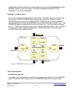

FPGA design
Cypress FX-2 LP and USB basics
Several data transfer types are defined in USB 2.0 specification. High-speed bulk transfer
is the one and only mode of interest to end users. USB transfers are packet oriented and
have a time framing scheme. USB packets consist of USB protocol and user payload data.
Payload could have a variable length of up to 512 bytes per packet. Packet size is fixed to
the maximum value of 512 bytes for data communication with CESYS USB cards to
achieve highest possible data throughput. USB peripherals could have several logical
channels to the host. The data source/sink for each channel inside the USB peripheral is
called the USB endpoint. Each endpoint can be configured as “IN”- (channel direction:
peripheral => host) or “OUT”-endpoint (channel direction: host => peripheral) from host
side perspective. CESYS USB cards support two endpoints, one for each direction. FX-2
has an integrated USB SIE (Serial Interface Engine) handling USB protocol and
transferring user payload data to the appropriate endpoint. So end users do not have to
care about USB protocol in their own applications. FX-2 endpoints are realized as 2 kB
buffers. These buffers can be accessed over a FIFO-like interface with a 16 bit tristate data
bus by external hardware. External hardware acts as a master, polling FIFO flags, applying
read- and write-strobes and transferring data. Therefore this FX-2 data transfer mechanism
is called “slave FIFO mode”. As already mentioned, all data is transferred in multiples of
512 bytes. External hardware has to ensure, that the data written to IN-endpoint is aligned
to this value, so that data will be transmitted from endpoint buffer to host. The 512 byte
alignment normally causes no restrictions in data streaming applications with endless data
transfers. Maybe it is necessary to fill up endpoint buffer with dummy data, if some kind of
host timeout condition has to be met. Another FX-2 data transfer mechanism is called
“GPIF (General Programmable InterFace) mode”. The GPIF engine inside the FX-2 acts as
a master to endpoint buffers, transferring data and presenting configurable handshake
waveforms to external hardware. CESYS USB card supports “slave FIFO mode” for data
communication only. “GPIF mode” is exclusively used for downloading configuration
bitstreams to FPGA.
Clocking FPGA designs
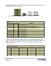
The 48 MHz SYSCLK oscillator is an onboard clock source for the FPGA. It is used as
interface clock (IFCLK) between FX-2 slave FIFO bus and FPGA I/Os. So this clock source
must be used for data transfers to and from FPGA over USB! Appropriate timing
constraints can be found in “*.ucf”-files of design examples included in delivery.
It is strictly recommended to use a single clock domain whenever possible. Using a fully
synchronous system architecture often results in smaller, less complex and more
performant FPGA designs (compare Xilinx
TM
white paper WP331 “Timing Closure/Coding
Guidelines”).
USBS6 / C1030-5510 http://www.cesys.com/
User Doc V0.3 -17- preliminary