


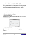

Register entry
A register entry can be used to communicate with a 32 bit register inside the FPGA. In
UDKLab, a register consists of the following values:
• Address
• Name
• Info text
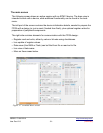
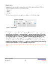
The visual representation of one register can be seen in the following image:
Figure 18: Register panel
The left buttons are responsible for adding new entries, move the entry up or down and
removing the current entry, all are self explanatory. The header shows it's mapping name
as well as the 32 bit address. The question mark in the lower right will show a tooltip if the
mouse is above it, which is just a little help for users. Both input fields can be used to write
in a new value, either hex- or decimal or contain the values if they are read from FPGA
design. The checkboxes represent one bit of the current value. Clicking the Read button
will read the current value from FPGA and update both text boxes as well as the
checkboxes, which is automatically done every 100ms if the Auto button is active. Setting
register values inside the FPGA is done in a similar way, clicking the Write button writes the
current values to the device. One thing needs a bit attention here:
Clicking on the checkboxes implicitly writes the value without the need to click on the Write
button !
USBS6 / C1030-5510 http://www.cesys.com/
User Doc V0.3 -58- preliminary