


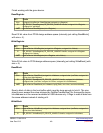
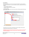
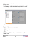
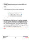

FPGA design flashing
This option stores a design into the flash component on devices that have support for it.
The design is loaded to the FPGA after device power on without host intervention. How
and under which circumstances this is done can be found in the hardware description of
the corresponding device. The following screen shows the required actions for flashing:
Figure 14: Flash design to device
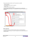
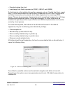
Projects
Device communication is placed into a small project management. This reduces the
actions from session to session and can be used for simple service tasks too. A projects
stores the following information:
• Device type it is intended to
• Initializing sequence
• Register list
• Data area list
Projects are handled like files in usual applications, they can be loaded, saved, new
USBS6 / C1030-5510 http://www.cesys.com/
User Doc V0.3 -54- preliminary