


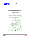
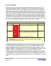
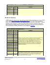
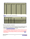

USB2.0 FX2LP
TM
Microcontroller CYPRESS
TM
CY7C68013A
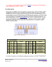
Signal Name FPGA IO Comment
FX2_FD11 U13
FX2_FD12 V13
FX2_FD13 U10
FX2_FD14 R8
FX2_FD15 T8
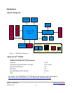
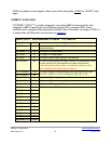
External memory
USBS6 offers the opportunity to use various external memory architectures in one´s FPGA
design. With Micron Technology MT46H64M16LFCK-5 up to 1Gbit of high-speed low-
power DDR SDRAM is available. The integrated memory controller of Spartan-6
TM
devices
enables system designers to implement state-of-the-art memory interfaces without the
need to develop a whole memory controller Soft-IP all on their own. Some examples on
how to implement LPDDR with Spartan-6 are available in chapter C.
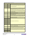
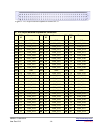
LPDDR SDRAM MT46H64M16LFCK-5
Signal Name FPGA IO Comment
MCB1_A0 H15
Address inputs: Provide the row address for ACTIVE commands, and
the column address and auto precharge bit (A10) for READ or
WRITE commands, to select one location out of the memory array in
the respective bank. During a PRECHARGE command, A10
determines whether the PRECHARGE applies to one bank (A10
LOW, bank selected by BA0, BA1) or all banks (A10 HIGH). The
address inputs also provide the op-code during a LOAD MODE
REGISTER command.
MCB1_A1 H16
MCB1_A2 F18
MCB1_A3 J13
MCB1_A4 E18
MCB1_A5 L12
MCB1_A6 L13
MCB1_A7 F17
MCB1_A8 H12
MCB1_A9 G13
MCB1_A10 E16
MCB1_A11 G14
MCB1_A12 D18
MCB1_A13 C17
MCB1_BA0 H13 Bank address inputs: BA0 and BA1 define to which bank an ACTIVE,
READ, WRITE, or PRECHARGE command is being applied. BA0
and BA1 also determine which mode register is loaded during a
LOAD MODE REGISTER command.
MCB1_BA1 H14
USBS6 / C1030-5510 http://www.cesys.com/
User Doc V0.3 -9- preliminary