


AD9912
Rev. D | Page 14 of 40
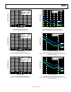
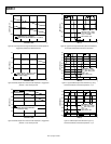
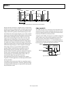
06763-021
0 200 400 600 800
FREQUENCY (MHz)
650
600
550
500
450
AMPLITUDE (mV)
NOM SKEW 25°C, 1.8V SUPPLY
WORST CASE (SLOW SKEW 90°C, 1.7V SUPPLY)
Figure 27. HSTL Output Driver Single-Ended Peak-to-Peak Amplitude vs.
Toggle Rate (100 Ω Across Differential Pair)
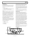
06763-022
0 10 20 30 40
FREQUENCY (MHz)
2.5
2.0
1.5
1.0
0.5
0
AMPLITUDE (V)
NOM SKEW 25°C, 1.8V SUPPLY (20pF)
WORST CASE (SLOW SKEW 90°C,
1.7V SUPPLY (20pF))
Figure 28. CMOS Output Driver Peak-to-Peak Amplitude vs. Toggle Rate
(AVDD3 = 1.8 V) with 20 pF Load
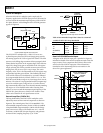
06763-023
0 50 100 150
FREQUENCY (MHz)
3.5
3.0
2.5
2.0
1.5
1.0
0.5
0
AMPLITUDE (V)
NOM SKEW 25°C, 1.8V SUPPLY (20pF)
WORST CASE (SLOW SKEW 90°C,
3.0V SUPPLY (20pF))
Figure 29. CMOS Output Driver Peak-to-Peak Amplitude vs. Toggle Rate
(AVDD3 = 3.3 V) with 20 pF Load
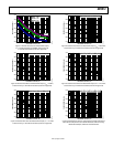
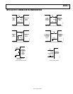
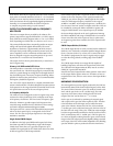
06763-024
0 0.5 1.0 1.5 2.0 2.5
TIME (ns)
0.4
0.6
0.2
0
–0.2
–0.4
–0.6
AMPLITUDE (V)
FREQUENCY = 600MHz
t
RISE
(20%→80%) = 104ps
t
FALL
(80%→20%) = 107ps
V p-p = 1.17V DIFF.
DUTY CYCLE = 50%
Figure 30. Typical HSTL Output Waveform, Nominal Conditions,
DC-Coupled, Differential Probe Across 100 Ω load
06763-025
0 20 40 60 80 100
TIME (ns)
1.8
1.6
1.4
1.2
1.0
0.8
0.6
0.4
0.2
0
–0.2
AMPLITUDE (V)
FREQUENCY = 20MHz
t
RISE
(20%→80%) = 5.5ns
t
FALL
(80%→20%) = 5.9ns
V p-p = 1.8V
DUTY CYCLE = 53%
Figure 31. Typical CMOS Output Driver Waveform (@ 1.8 V),
Nominal Conditions, Estimated Capacitance = 5 pF
06763-026
0 10 20 30 40 50
TIME (ns)
3.3
2.8
2.3
1.8
1.3
0.8
0.3
–0.2
AMPLITUDE (V)
FREQUENCY = 40MHz
t
RISE
(20%→80%) = 2.25ns
t
FALL
(80%→20%) = 2.6ns
V p-p = 3.3V
DUTY CYCLE = 52%
Figure 32. CMOS Output Driver Waveform (@ 3.3 V),
Nominal Conditions, Estimated Capacitance = 5 pF