


AD9912
Rev. D | Page 20 of 40
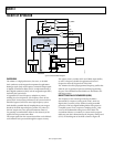
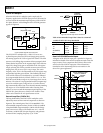
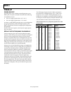
SYSCLK PLL Multiplier
When the SYSCLK PLL multiplier path is employed, the
frequency applied to the SYSCLK input pins must be limited so
as not to exceed the maximum input frequency of the SYSCLK
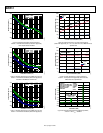
PLL phase detector. A block diagram of the SYSCLK generator
appears in Figure 45.
06763-037
PHASE
FREQUENCY
DETECTOR
CHARGE
PUMP
VCO
÷2÷N
~2pF
(N = 2 TO 33)
K
VCO
(HIGH/LOW RANGE)
2
I
CP
(125µA, 250µA, 375µA)
SYSCLK PLL MULTIPLIER
LOOP_FILTER
FROM
SYSCLK
INPUT
DAC
SAMPLE
CLOCK
1GHz
Figure 45. Block Diagram of the SYSCLK PLL
The SYSCLK PLL multiplier has a 1 GHz VCO at its core.
A phase/frequency detector (PFD) and charge pump provide
the steering signal to the VCO in typical PLL fashion. The PFD
operates on the falling edge transitions of the input signal, which
means that the loop locks on the negative edges of the reference
signal. The charge pump gain is controlled via the I/O register
map by selecting one of three possible constant current sources
ranging from 125 μA to 375 μA in 125 μA steps. The center
frequency of the VCO is also adjustable via the I/O register map
and provides high/low gain selection. The feedback path from
VCO to PFD consists of a fixed divide-by-2 prescaler followed
by a programmable divide-by-N block, where 2 ≤ N ≤ 33. This
limits the overall divider range to any even integer from 4 to 66,
inclusive. The value of N is programmed via the I/O register map
via a 5-bit word that spans a range of 0 to 31, but the internal
logic automatically adds a bias of 2 to the value entered, extending
the range to 33. Care should be taken when choosing these
values so as not to exceed the maximum input frequency of the
SYSCLK PLL phase detector or SYSCLK PLL doubler. These
values can be found in the AC Specifications section.
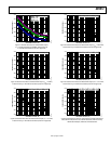
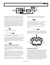
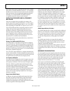
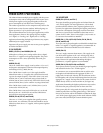
External Loop Filter (SYSCLK PLL)
The loop bandwidth of the SYSCLK PLL multiplier can be
adjusted by means of three external components as shown in
Figure 46. The nominal gain of the VCO is 800 MHz/V. The
recommended component values (shown in Table 6) establish
a loop bandwidth of approximately 1.6 MHz with the charge
pump current set to 250 μA. The default case is N = 40, and
it assumes a 25 MHz SYSCLK input frequency and generates
an internal DAC sampling frequency (f
S
) of 1 GHz.
06763-038
CHARGE
PUMP
~2pF
LOOP_FILTER
C2
R1
C1
EXTERNAL
LOOP FILTER
VCO
AD9912
FERRITE
BEAD
AVDD
29
26 31
Figure 46. External Loop Filter for SYSCLK PLL
Table 6. Recommended Loop Filter Values for a Nominal
1.5 MHz SYSCLK PLL Loop Bandwidth
Multiplier R1 Series C1 Shunt C2
<8 390 Ω 1 nF 82 pF
10 470 Ω 820 pF 56 pF
20 1 kΩ 390 pF 27 pF
40 (default) 2.2 kΩ 180 pF 10 pF
60 2.7 kΩ 120 pF 5 pF
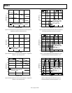
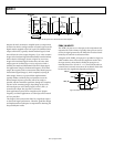
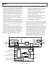
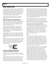
Detail of SYSCLK Differential Inputs
A diagram of the SYSCLK input pins is provided in Figure 47.
Included are details of the internal components used to bias the
input circuitry. These components have a direct effect on the
static levels at the SYSCLK input pins. This information is
intended to aid in determining how best to interface to the
device for a given application.
06763-039
500Ω
500Ω~1.5pF
~1.5pF
INTERNAL
CLOCK
V
SS
~1V
V
SS
~2pF
+
SYSCLK PLL BYPASSED
1kΩ
1kΩ~3pF
~3pF
INTERNAL
CLOCK
V
SS
~1V
V
SS
~2pF
+
SYSCLK PLL ENABLED
AMP
INTERNAL
CLOCK
CRYSTAL RESONATOR WITH
SYSCLK PLL ENABLED
MUX
SYSCLK
SYSCLKB
Figure 47. Differential SYSCLK Inputs