


AD9912
Rev. D | Page 27 of 40
Read
If the instruction word is for a read operation (I15 = 1), the next
N × 8 SCLK cycles clock out the data from the address specified
in the instruction word, where N is 1, 2, 3, or 4, as determined
by [W1:W0]. In this case, 4 is used for streaming mode where
four or more words are transferred per read. The data readback
is valid on the falling edge of SCLK.
The default mode of the AD9912 serial control port is bidirec-
tional mode, and the data readback appears on the SDIO pin. It
is possible to set the AD9912 to unidirectional mode by writing
to the SDO active bit (Register 0x0000, Bit 0 = 1), and in that
mode, the requested data appears on the SDO pin.
By default, a read request reads the register value that is cur-
rently in use by the AD9912. However, setting Register 0x0004,
Bit 0 = 1 causes the buffered registers to be read instead. The
buffered registers are the ones that take effect during the next
I/O update.
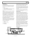
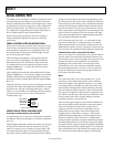
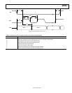
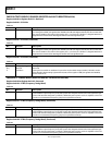
06763-042
AD9912
CORE
UPDATE
REGISTERS
TOGGLE
IO_UPDATE
PIN
SCLK
SDIO
SDO
CSB
SERIAL
CONTROL
PORT
CONTROL REGISTERS
REGISTER BUFFERS
Figure 50. Relationship Between Serial Control Port Register Buffers and
Control Registers of the AD9912
The AD9912 uses Register 0x0000 to Register 0x0509. Although
the AD9912 serial control port allows both 8-bit and 16-bit
instructions, the 8-bit instruction mode provides access to five
address bits (A4 to A0) only, which restricts its use to Address
Space 0x00 to Address Space 0x31. The AD9912 defaults to 16-bit
instruction mode on power-up, and the 8-bit instruction mode
is not supported.
THE INSTRUCTION WORD (16 BITS)
The MSB of the instruction word is R/
W
For a write, the instruction word is followed by the number of
bytes of data indicated by Bits[W1:W0], which is interpreted
according to
, which indicates
whether the instruction is a read or a write. The next two bits,
[W1:W0], are the transfer length in bytes. The final 13 bits are
the address ([A12:A0]) at which to begin the read or write
operation.
Table 9.
Bits[A12:A0] select the address within the register map that is
written to or read from during the data transfer portion of the
communications cycle. The AD9912 uses all of the 13-bit
address space. For multibyte transfers, this address is the
starting byte address.
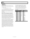
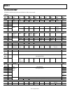
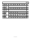
Table 9. Byte Transfer Count
W1 W0
Bytes to Transfer
(Excluding the 2-Byte Instruction)
0 0 1
0 1 2
1 0 3
1 1 Streaming mode
MSB/LSB FIRST TRANSFERS
The AD9912 instruction word and byte data can be MSB first or
LSB first. The default for the AD9912 is MSB first. The LSB first
mode can be enabled by writing a 1 to the LSB first bit in the
serial configuration register and then issuing an I/O update.
Immediately after the LSB first bit is set, all serial control port
operations are changed to LSB first order.
When MSB first mode is active, the instruction and data bytes
must be written from MSB to LSB. Multibyte data transfers in
MSB first format start with an instruction byte that includes the
register address of the most significant data byte. Subsequent
data bytes must follow in order from high address to low address.
In MSB first mode, the serial control port internal address
generator decrements for each data byte of the multibyte
transfer cycle.
When LSB first = 1 (LSB first), the instruction and data bytes
must be written from LSB to MSB. Multibyte data transfers in
LSB first format start with an instruction byte that includes the
register address of the least significant data byte followed by
multiple data bytes. The serial control port internal byte address
generator increments for each byte of the multibyte transfer cycle.
The AD9912 serial control port register address decrements from
the register address just written toward 0x0000 for multibyte
I/O operations if the MSB first mode is active (default). If the
LSB first mode is active, the serial control port register address
increments from the address just written toward 0x1FFF for
multibyte I/O operations.
Unused addresses are not skipped during multibyte I/O operations.
The user should write the default value to a reserved register and
should write only zeros to unmapped registers. Note that it is
more efficient to issue a new write command than to write the
default value to more than two consecutive reserved (or
unmapped) registers.