


AD9912
Rev. D | Page 33 of 40
Register 0x0011—Reserved
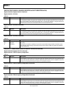
Register 0x0012—Reset (Autoclearing)
To reset the entire chip, the user can use the (non-autoclearing) soft reset bit in Register 0x0000.
Table 17.
Bits Bit Name Description
0 DDS reset Reset of the direct digital synthesis block. Reset of this block is very seldom needed.
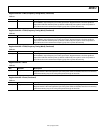
Register 0x0013—Reset (Continued) (Not Autoclearing)
Table 18.
Bits Bit Name Description
7 PD fund DDS Setting this bit powers down the DDS fundamental output but not the spurs. It is used during tuning
of the SpurKiller circuit.
3 S-div/2 reset Asynchronous reset for S prescaler.
1 S-divider reset Synchronous (to S-divider prescaler output) reset for integer divider.
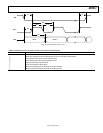
SYSTEM CLOCK (REGISTER 0x0020 TO REGISTER 0x0022)
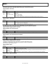
Register 0x0020—N-Divider
Table 19.
Bits Bit Name Description
[4:0] N-divider These bits set the feedback divider for system clock PLL. There is a fixed divide-by-2 preceding this
block, as well as an offset of 2 added to this value. Therefore, setting this register to 00000 translates to
an overall feedback divider ratio of 4. See Figure 45.
Register 0x0021—Reserved
Register 0x0022—PLL Parameters
Table 20.
Bits Bit Name Description
7 VCO auto range Automatic VCO range selection. Enabling this bit allows Bit 2 of this register to be set automatically.
[6:4] Reserved Reserved.
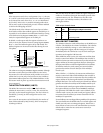
3 2× reference Enables a frequency doubler prior to the SYSCLK PLL and can be useful in reducing jitter induced by
the SYSCLK PLL. See Figure 44.
2 VCO range Selects low range or high range VCO.
0 = low range (700 MHz to 810 MHz).
1 = high range (900 MHz to 1000 MHz). For system clock settings between 810 MHz and 900 MHz, use
the VCO auto range (Bit 7) to set the correct VCO range automatically.
[1:0] Charge pump current Charge pump current.
00 = 250 μA.
01 = 375 μA.
10 = off.
11= 125 μA.