


AD9912
Rev. D | Page 4 of 40
Parameter Min Typ Max Unit Test Conditions/Comments
SYSTEM CLOCK INPUT System clock inputs should always be ac-
coupled (both single-ended and differential)
SYSCLK PLL Bypassed
Input Capacitance 1.5 pF Single-ended, each pin
Input Resistance 2.4 2.6 2.9 kΩ Differential
Internally Generated DC Bias Voltage
2
0.93 1.17 1.38 V
Differential Input Voltage Swing 632 mV p-p Equivalent to 316 mV swing on each leg
SYSCLK PLL Enabled
Input Capacitance 3 pF Single-ended, each pin
Input Resistance 2.4 2.6 2.9 kΩ Differential
Internally Generated DC Bias Voltage
2
0.93 1.17 1.38 V
Differential Input Voltage Swing 632 mV p-p Equivalent to 316 mV swing on each leg
Crystal Resonator with SYSCLK PLL Enabled
Motional Resistance 9 100 Ω 25 MHz, 3.2 mm × 2.5 mm AT cut
CLOCK OUTPUT DRIVERS
HSTL Output Driver
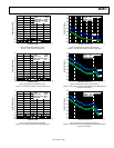
Differential Output Voltage Swing
1080 1280 1480 mV Output driver static, see Figure 27 for
output swing vs. frequency
Common-Mode Output Voltage
2
0.7 0.88 1.06 V
CMOS Output Driver Output driver static, see Figure 28 and
Figure 29 for output swing vs. frequency
Output Voltage High (V
OH
) 2.7 V I
OH
= 1 mA, Pin 37 = 3.3 V
Output Voltage Low (V
OL
) 0.4 V I
OL
= 1 mA, Pin 37 = 3.3 V
Output Voltage High (V
OH
) 1.4 V I
OH
= 1 mA, Pin 37 = 1.8 V
Output Voltage Low (V
OL
) 0.4 V I
OL
= 1 mA, Pin 37 = 1.8 V
TOTAL POWER DISSIPATION
DDS Only 637 765 mW Power-on default, except SYSCLK PLL by-
passed and CMOS driver off; SYSCLK = 1 GHz;
HSTL driver off; spur reduction off; f
OUT
=
200 MHz
DDS with Spur Reduction On 686 823 mW Same as “DDS Only” case, except both spur
reduction channels on
DDS with HSTL Driver Enabled 657 788 mW Same as “DDS Only” case, except HSTL driver
enabled
DDS with CMOS Driver Enabled 729 875 mW Same as “DDS Only” case, except CMOS
driver and S-divider enabled and at 3.3 V;
CMOS f
OUT
= 50 MHz (S-divider = 4)
DDS with HSTL and CMOS Drivers Enabled 747 897 mW Same as “DDS Only” case, except both HSTL
and CMOS drivers enabled; S-divider
enabled and set to 4; CMOS f
OUT
= 50 MHz
DDS with SYSCLK PLL Enabled 648 777 mW Same as “DDS Only” case, except 25 MHz on
SYCLK input and PLL multiplier = 40
Power-Down Mode 13 16 mW Using either the power-down and enable
register or the PWRDOWN pin
1
Pin 14 is in the AVDD3 group, but it is recommended that Pin 14 be tied to Pin 1.
2
AVSS = 0 V.