


AD9912
Rev. D | Page 26 of 40
SERIAL CONTROL PORT
The AD9912 serial control port is a flexible, synchronous, serial
communications port that allows an easy interface with many
industry-standard microcontrollers and microprocessors. Single
or multiple byte transfers are supported, as well as MSB first or
LSB first transfer formats. The AD9912 serial control port can
be configured for a single bidirectional I/O pin (SDIO only) or
for two unidirectional I/O pins (SDIO and SDO).
Note that all serial port operations (such as the frequency
tuning word update) depend on the presence of the DAC
system clock.
SERIAL CONTROL PORT PIN DESCRIPTIONS
SCLK (serial clock) is the serial shift clock. This pin is an input.
SCLK is used to synchronize serial control port reads and writes.
Write data bits are registered on the rising edge of this clock,
and read data bits are registered on the falling edge. This pin
has an internal pull-down resistor.
SDIO (serial data input/output) is a dual-purpose pin and
acts as input only or input/output. The AD9912 defaults to
bidirectional pins for I/O. Alternatively, SDIO can be used
as a unidirectional I/O pin by writing to the SDO active bit
(Register 0x0000, Bit 0 = 1). In this case, SDIO is the input,
and SDO is the output.
SDO (serial data out) is used only in the unidirectional I/O mode
(Register 0x0000, Bit 0 = 1) as a separate output pin for reading
back data. Bidirectional I/O mode (using SDIO as both input
and output) is active by default (SDO active bit: Register 0x0000,
Bit 0 = 0).
CSB (chip select bar) is an active low control that gates the read
and write cycles. When CSB is high, SDO and SDIO are in a high
impedance state. This pin is internally pulled up by a 100 kΩ
resistor to 3.3 V. It should not be left floating. See the Operation
of Serial Control Port section on the use of the CSB in a
communication cycle.
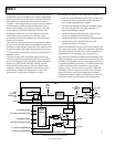
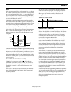
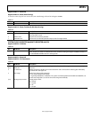
06763-041
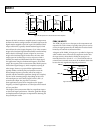
AD9912
SERIAL
CONTROL
PORT
SCLK (PIN 64)
SDIO (PIN 63)
SDO (PIN 62)
CSB (PIN 61)
Figure 49. Serial Control Port
OPERATION OF SERIAL CONTROL PORT
Framing a Communication Cycle with CSB
A communication cycle (a write or a read operation) is gated by
the CSB line. CSB must be brought low to initiate a communica-
tion cycle.
CSB stall high is supported in modes where three or fewer bytes
of data (plus the instruction data) are transferred ([W1:W0]
must be set to 00, 01, or 10; see Table 9). In these modes, CSB
can temporarily return high on any byte boundary, allowing
time for the system controller to process the next byte. CSB can
go high on byte boundaries only and can go high during either
part (instruction or data) of the transfer. During this period, the
serial control port state machine enters a wait state until all data
has been sent. If the system controller decides to abort the transfer
before all of the data is sent, the state machine must be reset by
either completing the remaining transfer or by returning the CSB
low for at least one complete SCLK cycle (but fewer than eight
SCLK cycles). Raising the CSB on a nonbyte boundary terminates
the serial transfer and flushes the buffer.
In the streaming mode ([W1:W0] = 11), any number of data
bytes can be transferred in a continuous stream. The register
address is automatically incremented or decremented (see the
MSB/LSB First Transfers section). CSB must be raised at the end
of the last byte to be transferred, thereby ending the stream mode.
Communication Cycle—Instruction Plus Data
There are two parts to a communication cycle with the AD9912.
The first writes a 16-bit instruction word into the AD9912, coin-
cident with the first 16 SCLK rising edges. The instruction word
provides the AD9912 serial control port with information
regarding the data transfer, which is the second part of the
communication cycle. The instruction word defines whether
the upcoming data transfer is a read or a write, the number of
bytes in the data transfer, and the starting register address for
the first byte of the data transfer.
Write
If the instruction word is for a write operation (I15 = 0), the
second part is the transfer of data into the serial control port
buffer of the AD9912. The length of the transfer (1, 2, or 3 bytes,
or streaming mode) is indicated by two bits ([W1:W0]) in the
instruction byte. The length of the transfer indicated by [W1:W0]
does not include the 2-byte instruction. CSB can be raised after
each sequence of eight bits to stall the bus (except after the last
byte, where it ends the cycle). When the bus is stalled, the serial
transfer resumes when CSB is lowered. Stalling on nonbyte
boundaries resets the serial control port.
There are three types of registers on the AD9912: buffered, live,
and read only. Buffered (also referred to as mirrored) registers
require an I/O update to transfer the new values from a
temporary buffer on the chip to the actual register and are
marked with an M in the Type column of the register map.
Toggling the IO_UPDATE pin or writing a 1 to the register
update bit (Register 0x0005, Bit 0) causes the update to occur.
Because any number of bytes of data can be changed before
issuing an update command, the update simultaneously enables
all register changes that have occurred since any previous update.
Live registers do not require I/O update; they update immediately
after being written. Read-only registers ignore write commands
and are marked RO in the Type column of the register map. An
AC in this column indicates that the register is autoclearing.