


AD9912
Rev. D | Page 24 of 40
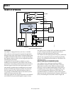
POWER-UP
POWER-ON RESET
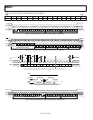
On initial power-up, the AD9912 internally generates a 75 ns
RESET pulse. The pulse is initiated when both of the following
two conditions are met:
• The 3.3 V supply is greater than 2.35 V ± 0.1 V.
• The 1.8 V supply is greater than 1.4 V ± 0.05 V.
Less than 1 ns after RESET goes high, the S1 to S4 configuration
pins go high impedance and remain high impedance until
RESET is deactivated. This allows strapping and configuration
during RESET.
Because of this reset sequence, external power supply sequenc-
ing is not critical.
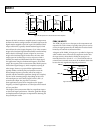
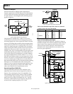
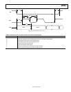
DEFAULT OUTPUT FREQUENCY ON POWER-UP
The four status pins (S1 to S4) are used to define the output
frequency of the DDS at power-up even though the I/O registers
have not yet been programmed. At power-up, internal logic
initiates a reset pulse of about 10 ns. During this time, S1 to S4
briefly function as input pins and can be driven externally. Any
logic levels thus applied are transferred to a 4-bit register on the
falling edge of the internally initiated pulse. The same behavior
occurs when the RESET pin is asserted manually.
Setting up S1 to S4 for default DDS startup is accomplished by
connecting a resistor to each pin (either pull-up or pull-down)
to produce the desired bit pattern, yielding 16 possible states
that are used both to address an internal 8 × 16 ROM and to
select the SYSCLK mode (see Table 8). The ROM contains eight
16-bit DDS frequency tuning words (FTWs), one of which is
selected by the state of the S1 to S3 pins. The selected FTW is
transferred to the FTW0 register in the I/O register map
without the need for an I/O update. This ensures that the DDS
generates the selected frequency even if the I/O registers have
not been programmed. The state of the S4 pin selects whether
the internal system clock is generated by means of the internal
SYSCLK PLL multiplier or not (see the SYSCLK Inputs section
for details).
The DDS output frequency listed in Table 8 assumes that
the internal DAC sampling frequency (f
S
) is 1 GHz. These
frequencies scale 1:1 with f
S
, meaning that other start-up
frequencies are available by varying the SYSCLK frequency.
At startup, the internal frequency multiplier defaults to 40×
when the Xtal/PLL mode is selected via the status pins.
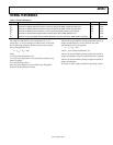
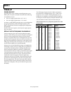
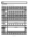
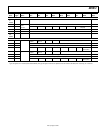
Table 8. Default Power-Up Frequency Options for 1 GHz
System Clock
Status Pin
SYSCLK
Input Mode
Output Frequency
(MHz)
S4 S3 S2 S1
0 0 0 0 Xtal/PLL 0
0 0 0 1 Xtal/PLL 38.87939
0 0 1 0 Xtal/PLL 51.83411
0 0 1 1 Xtal/PLL 61.43188
0 1 0 0 Xtal/PLL 77.75879
0 1 0 1 Xtal/PLL 92.14783
0 1 1 0 Xtal/PLL 122.87903
0 1 1 1 Xtal/PLL 155.51758
1 0 0 0 Direct 0
1 0 0 1 Direct 38.87939
1 0 1 0 Direct 51.83411
1 0 1 1 Direct 61.43188
1 1 0 0 Direct 77.75879
1 1 0 1 Direct 92.14783
1 1 1 0 Direct 122.87903
1 1 1 1 Direct 155.51758