


AD9912
Rev. D | Page 36 of 40
DOUBLER AND OUTPUT DRIVERS (REGISTER 0x0200 TO REGISTER 0x0201)
Register 0x0200—HSTL Driver
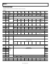
Table 32.
Bits Bit Name Description
4 OPOL Output polarity. Setting this bit inverts the HSTL driver output polarity.
[3:2] Reserved Reserved.
[1:0] HSTL output doubler HSTL output doubler.
01 = doubler disabled.
10 = doubler enabled. When using doubler, Bit 5 in Register 0x0010 must also be set to 1.
Register 0x0201—CMOS Driver
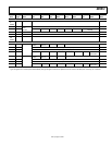
Table 33.
Bits Bit Name Description
0 CMOS mux This bit allows the user to select whether the CMOS driver output is divided by the S-divider.
0 = S-divider input sent to CMOS driver.
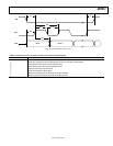
1 = S-divider output sent to CMOS driver. See Figure 39.
CALIBRATION (USER-ACCESSIBLE TRIM) (REGISTER 0x0400 TO REGISTER 0x0410)
Register 0x0400 to Register 0x040A—Reserved
Register 0x040B—DAC Full-Scale Current
Table 34.
Bits Bit Name Description
[7:0] DAC full-scale current DAC full-scale current, Bits[7:0]. See the Digital-to-Analog (DAC) Output section.
Register 0x040C—DAC Full-Scale Current (Continued)
Table 35.
Bits Bit Name Description
[9:8] DAC full-scale current DAC full-scale current, Bits[9:8]. See Register 0x040B.
Register 0x040D to Register 0x0410—Reserved
HARMONIC SPUR REDUCTION (REGISTER 0x0500 TO REGISTER 0x0509)
See the Harmonic Spur Reduction section.
Register 0x0500—Spur A
Table 36.
Bits Bit Name Description
7 HSR-A enable Harmonic Spur Reduction A enable.
6 Amplitude gain × 2 Setting this bit doubles the gain of the cancelling circuit and also doubles the minimum step size.
[5:4] Reserved Reserved.
[3:0] Spur A harmonic Spur A Harmonic 1 to Spur A Harmonic 15. Allows user to choose which harmonic to eliminate.
Register 0x0501—Spur A (Continued)
Table 37.
Bits Bit Name Description
[7:0] Spur A magnitude Linear multiplier for Spur A magnitude.