


AD9912
Rev. D | Page 19 of 40
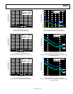
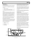
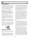
SYSCLK INPUTS
Functional Description
An external time base connects to the AD9912 at the SYSCLK
pins to generate the internal high frequency system clock (f
S
).
The SYSCLK inputs can be operated in one of the following
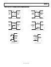
three modes:
• SYSCLK PLL bypassed
• SYSCLK PLL enabled with input signal generated externally
• Crystal resonator with SYSCLK PLL enabled
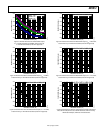
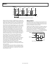
A functional diagram of the system clock generator is shown in
Figure 44.
The SYSCLK PLL multiplier path is enabled by a Logic 0 (default)
in the PD SYSCLK PLL bit (Register 0x0010, Bit 4) of the I/O
register map. The SYSCLK PLL multiplier can be driven from
the SYSCLK input pins by one of two means, depending on the
logic level applied to the 1.8 V CMOS CLKMODESEL pin.
When CLKMODESEL = 0, a crystal can be connected directly
across the SYSCLK pins. When CLKMODESEL = 1, the
maintaining amp is disabled, and an external frequency source
(such as an oscillator or signal generator) can be connected
directly to the SYSCLK input pins. Note that CLKMODESEL = 1
does not disable the system clock PLL.
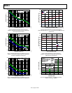
The maintaining amp on the AD9912 SYSCLK pins is intended
for 25 MHz, 3.2 mm × 2.5 mm AT cut fundamental mode crystals
with a maximum motional resistance of 100 Ω. The following
crystals, listed in alphabetical order, meet these criteria (as of
the revision date of this data sheet):
• AVX/Kyocera CX3225SB
• ECS ECX-32
• Epson/Toyocom TSX-3225
• Fox FX3225BS
• NDK NX3225SA
Note that although these crystals meet the preceding criteria
according to their data sheets, Analog Devices, Inc., does not
guarantee their operation with the AD9912, nor does Analog
Devices endorse one supplier of crystals over another.
When the SYSCLK PLL multiplier path is disabled, the AD9912
must be driven by a high frequency signal source (250 MHz to
1 GHz). The signal thus applied to the SYSCLK input pins becomes
the internal DAC sampling clock (f
S
) after passing through an
internal buffer.
It is important to note that when bypassing the system clock
PLL, the LOOP_FILTER pin (Pin 31) should be pulled down to
the analog ground with a 1 kΩ resistor.
SYSCLK PLL Doubler
The SYSCLK PLL multiplier path offers an optional SYSCLK
PLL doubler. This block comes before the SYSCLK PLL
multiplier and acts as a frequency doubler by generating a pulse
on each edge of the SYSCLK input signal. The SYSCLK PLL
multiplier locks to the falling edges of this regenerated signal.
The impetus for doubling the frequency at the input of the
SYSCLK PLL multiplier is that an improvement in overall phase
noise performance can be realized. The main drawback is that
the doubler output is not a rectangular pulse with a constant
duty cycle even for a perfectly symmetric SYSCLK input signal.
This results in a subharmonic appearing at the same frequency
as the SYSCLK input signal, and the magnitude of the subharmonic
can be quite large. When employing the doubler, care must be
taken to ensure that the loop bandwidth of the SYSCLK PLL
multiplier adequately suppresses the subharmonic.
The benefit offered by the doubler depends on the magnitude
of the subharmonic, the loop bandwidth of the SYSCLK PLL
multiplier, and the overall phase noise requirements of the
specific application. In many applications, the AD9912 clock
output is applied to the input of another PLL, and the subhar-
monic is often suppressed by the relatively narrow bandwidth of
the downstream PLL.
Note that generally, the benefits of the SYSCLK PLL doubler are
realized for SYSCLK input frequencies of 25 MHz and above.
06763-036
1
0
1
0
1
0
BIPOLAR
EDGE
DETECTOR
2
2
WITH CRYSTAL
RESONATOR
2
2
1
0
2
2
2
SYSCLK
PLL
ENABLED
WITH EXTERNAL DRIVE
SYSCLK PLL BYPASSED
SYSCLK
PLL
MULTIPLIER
1
0
BIPOLAR EDGE DETECTOR
(I/O REGISTER BIT)
PD SYSCLK PLL
(I/O REGISTER BIT)
DAC
SAMPLE
CLOCK
LOOP_FILTER
SYSCLK
SYSCLKB
CLKMODESEL
2
Figure 44. System Clock Generator Block Diagram