


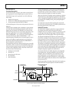

AD9912
Rev. D | Page 23 of 40
THERMAL PERFORMANCE
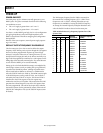
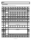
Table 7. Thermal Parameters
Symbol Thermal Characteristic Using a JEDEC51-7 Plus JEDEC51-5 2S2P Test Board Value Unit
θ
JA
Junction-to-ambient thermal resistance, 0.0 m/sec air flow per JEDEC JESD51-2 (still air) 25.2 °C/W
θ
JMA
Junction-to-ambient thermal resistance, 1.0 m/sec air flow per JEDEC JESD51-6 (moving air) 22.0 °C/W
θ
JMA
Junction-to-ambient thermal resistance, 2.0 m/sec air flow per JEDEC JESD51-6 (moving air) 19.8 °C/W
θ
JB
Junction-to-board thermal resistance, 1.0 m/sec air flow per JEDEC JESD51-8 (moving air) 13.9 °C/W
θ
JC
Junction-to-case thermal resistance (die-to-heat sink) per MIL-Std 883, Method 1012.1 1.7 °C/W
Ψ
JT
Junction-to-top-of-package characterization parameter, 0 m/sec air flow per JEDEC JESD51-2 (still air) 0.1 °C/W
The AD9912 is specified for a case temperature (T
CASE
). To
ensure that T
CASE
is not exceeded, an airflow source can be used.
Use the following equation to determine the junction tempera-
ture on the application PCB:
T
J
= T
CASE
+ (Ψ
JT
× PD)
where:
T
J
is the junction temperature (°C).
T
CASE
is the case temperature (°C) measured by customer at top
center of package.
Ψ
JT
is the value from Table 7.
PD is the power dissipation (see the Total Power Dissipation
section in the Specifications section).
Values of θ
JA
are provided for package comparison and PCB
design considerations. θ
JA
can be used for a first-order
approximation of T
J
by the equation
T
J
= T
A
+ (θ
JA
× PD)
where T
A
is the ambient temperature (°C).
Values of θ
JC
are provided for package comparison and PCB
design considerations when an external heat sink is required.
Values of θ
JB
are provided for package comparison and PCB
design considerations.
The values in Table 7 apply to both 64-lead package options.