


AD9912
Rev. D | Page 17 of 40
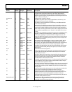
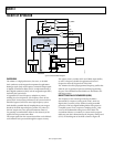
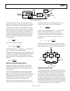
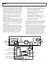
06763-032
DAC
(14-BIT)
ANGLE TO
AMPLITUDE
CONVERSION
1419
194848
48
14
PHASE
OFFSET
QD
48-BIT ACCUMULATOR
FREQUENCY
TUNING WORD
(FTW)
f
S
DAC_RSET
DAC_OUT
DAC_OUTB
DAC I-SET
REGISTERS
AND LOGIC
Figure 40. DDS Block Diagram
The input to the DDS is a 48-bit FTW that provides the accu-
mulator with a seed value. On each cycle of f
S
, the accumulator
adds the value of the FTW to the running total of its output.
For example, given an FTW = 5, the accumulator increments
the count by 5 sec on each f
S
cycle. Over time, the accumulator
reaches the upper end of its capacity (2
48
in this case) and then
rolls over, retaining the excess. The average rate at which the
accumulator rolls over establishes the frequency of the output
sinusoid. The following equation defines the average rollover
rate of the accumulator and establishes the output frequency
(f
DDS
) of the DDS:
SDDS
f
FTW
f
=
48
2
Solving this equation for FTW yields
=
S
DDS
f
f
FTW
48
2round
For example, given that f
S
= 1 GHz and f
DDS
= 19.44 MHz, then
FTW = 5,471,873,547,255 (0x04FA05143BF7).
The relative phase of the sinusoid can be controlled numerically,
as well. This is accomplished using the phase offset function of
the DDS (a programmable 14-bit value (Δphase); see the I/O
Register Map section). The resulting phase offset, ΔΦ (radians),
is given by
∆
π=∆
14
2
2
phase
Φ
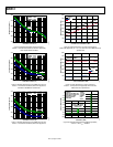
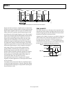
DIGITAL-TO-ANALOG (DAC) OUTPUT
The output of the digital core of the DDS is a time series of
numbers representing a sinusoidal waveform. This series is
translated to an analog signal by means of a digital-to-analog
converter (DAC).
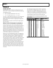
The DAC outputs its signal to two pins driven by a balanced
current source architecture (see the DAC output diagram in
Figure 41). The peak output current derives from a combination
of two factors. The first is a reference current (I
DAC_REF
) that is
established at the DAC_RSET pin, and the second is a scale
factor that is programmed into the I/O register map.
The value of I
DAC_REF
is set by connecting a resistor (R
DAC_REF
)
between the DAC_RSET pin and ground. The DAC_RSET pin
is internally connected to a virtual voltage reference of 1.2 V
nominal, so the reference current can be calculated by
REFDAC
REFDAC
R
I
_
_
2.1
=
Note that the recommended value of I
DAC_REF
is 120 μA, which
leads to a recommended value for R
DAC_REF
of 10 kΩ.
The scale factor consists of a 10-bit binary number (FSC)
programmed into the DAC full-scale current register in the
I/O register map. The full-scale DAC output current (I
DAC_FS
)
is given by
+=
1024
192
72
__
FSC
II
REFDACFSDAC
Using the recommended value of R
DAC_REF
, the full-scale DAC
output current can be set with 10-bit granularity over a range of
approximately 8.6 mA to 31.7 mA. 20 mA is the default value.
06763-033
SWITCH
CONTROL
CODE
I
FS
/2 I
FS
/2
AVDD3
AVSS
CURRENT
SWITCH
ARRAY
CURRENT
SWITCH
ARRAY
DAC_OUT
DAC_OUTB
INTERNAL
50Ω
INTERNAL
50Ω
I
FS
/2 + I
CODE
I
FS
/2 – I
CODE
I
FS
49
51
50
52
Figure 41. DAC Output
RECONSTRUCTION FILTER
The origin of the output clock signal produced by the AD9912
is the combined DDS and DAC. The DAC output signal appears
as a sinusoid sampled at f
S
. The frequency of the sinusoid is
determined by the frequency tuning word (FTW) that appears
at the input to the DDS. The DAC output is typically passed
through an external reconstruction filter that serves to remove
the artifacts of the sampling process and other spurs outside the
filter bandwidth. If desired, the signal can then be brought back
on-chip to be converted to a square wave that is routed internally
to the output clock driver or the 2× DLL multiplier.