


AD9912
Rev. D | Page 9 of 40
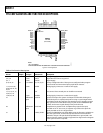
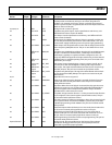
Pin No.
Input/
Output Pin Type Mnemonic Description
32 I 1.8 V CMOS CLKMODESEL Clock Mode Select. Set to GND when connecting a crystal to the system
clock input (Pin 27 and Pin 28). Pull up to 1.8 V when using either an
oscillator or an external clock source. This pin can be left unconnected
when the system clock PLL is bypassed. (See the SYSCLK Inputs section for
details on the use of this pin.)
33, 39, 43, 52 O GND AVSS Analog Ground. Connect to ground.
34 O 1.8 V HSTL OUTB Complementary HSTL Output. See the Specifications and Primary 1.8 V
Differential HSTL Driver sections for details.
35 O 1.8 V HSTL OUT HSTL Output. See the Specifications and Primary 1.8 V Differential HSTL
Driver sections for details.
37 I Power AVDD3 Analog Supply for CMOS Output Driver. This pin is normally 3.3 V but can
be 1.8 V. This pin should be powered even if the CMOS driver is not used.
See the Power Supply Partitioning section for power supply partitioning.
38 O 3.3 V CMOS OUT_CMOS CMOS Output. See the Specifications section and the Output Clock Drivers
and 2× Frequency Multiplier section. This pin is 1.8 V CMOS if Pin 37 is set
to 1.8 V.
40 I Differential
input
FDBK_INB Complementary Feedback Input. When using the HSTL and CMOS outputs,
this pin is connected to the filtered DAC_OUTB output. This internally
biased input is typically ac-coupled, and when configured as such, can
accept any differential signal whose single-ended swing is at least 400 mV.
41 I Differential
input
FDBK_IN Feedback Input. In standard operating mode, this pin is connected to the
filtered DAC_OUT output.
48 O Current set
resistor
DAC_RSET DAC Output Current Setting Resistor. Connect a resistor (usually 10 kΩ)
from this pin to GND. See the Digital-to-Analog (DAC) Output section.
50 O Differential
output
DAC_OUT DAC Output. This signal should be filtered and sent back on-chip through
the FDBK_IN input. This pin has an internal 50 Ω pull-down resistor.
51 O Differential
output
DAC_OUTB Complementary DAC Output. This signal should be filtered and sent back
on-chip through the FDBK_INB input. This pin has an internal 50 Ω pull-
down resistor.
56, 57 Power DVSS Digital Ground. Connect to ground.
58 I 3.3 V CMOS PWRDOWN Power-Down. When this active high pin is asserted, the device becomes
inactive and enters the full power-down state. This pin has an internal
50 kΩ pull-down resistor.
59 I 3.3 V CMOS RESET Chip Reset. When this active high pin is asserted, the chip goes into reset.
Note that on power-up, a 10 μs reset pulse is internally generated when
the power supplies reach a threshold and stabilize. This pin should be
grounded with a 10 kΩ resistor if not used.
60 I 3.3 V CMOS IO_UPDATE I/O Update. A logic transition from 0 to 1 on this pin transfers data from the
I/O port registers to the control registers (see the Write section). This pin
has an internal 50 kΩ pull-down resistor.
61 I 3.3 V CMOS CSB Chip Select. Active low. When programming a device, this pin must be held
low. In systems where more than one AD9912 is present, this pin enables
individual programming of each AD9912. This pin has an internal 100 kΩ
pull-up resistor.
62 O 3.3 V CMOS SDO Serial Data Output. When the device is in 3-wire mode, data is read on this
pin. There is no internal pull-up/pull-down resistor on this pin.
63 I/O 3.3 V CMOS SDIO Serial Data Input/Output. When the device is in 3-wire mode, data is
written via this pin. In 2-wire mode, data reads and writes both occur on
this pin. There is no internal pull-up/pull-down resistor on this pin.
64 I 3.3 V CMOS SCLK Serial Programming Clock. Data clock for serial programming. This pin has
an internal 50 kΩ pull-down resistor.
Exposed Die Pad O GND EPAD Analog Ground. The exposed die pad on the bottom of the package
provides the analog ground for the part; this exposed pad must be
connected to ground for proper operation.