


AD9912
Rev. D | Page 5 of 40
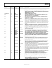
AC SPECIFICATIONS
f
S
= 1 GHz, DAC R
SET
= 10 kΩ, unless otherwise noted. Power supply pins within the range specified in the DC Specifications section.
Table 2.
Parameter Min Typ Max Unit Test Conditions/Comments
FDBK_IN INPUT Pin 40, Pin 41
Input Frequency Range 10 400 MHz
Minimum Differential Input Level 225 mV p-p −12 dBm into 50 Ω; must be ac-coupled
40 V/μs
SYSTEM CLOCK INPUT Pin 27, Pin 28
SYSCLK PLL Bypassed
Input Frequency Range 250 1000 MHz Maximum f
OUT
is 0.4 × f
SYSCLK
Duty Cycle 45 55 %
Minimum Differential Input Level 632 mV p-p Equivalent to 316 mV swing on each leg
SYSCLK PLL Enabled
VCO Frequency Range, Low Band 700 810 MHz When in the range, use the low VCO band exclusively
VCO Frequency Range, Auto Band 810 900 MHz When in the range, use the VCO auto band select
VCO Frequency Range, High Band 900 1000 MHz When in the range, use the high VCO band exclusively
Maximum Input Rate of System
Clock PFD
100 MHz
Without SYSCLK PLL Doubler
Input Frequency Range 11 200 MHz
Multiplication Range 4 66 Integer multiples of 2, maximum PFD rate and system clock
frequency must be met
Minimum Differential Input Level 632 mV p-p Equivalent to 316 mV swing on each leg
With SYSCLK PLL Doubler
Input Frequency Range 6 100 MHz
Multiplication Range 8 132 Integer multiples of 8
Input Duty Cycle 50 % Deviating from 50% duty cycle may adversely affect
spurious performance
Minimum Differential Input Level 632 mV p-p Equivalent to 316 mV swing on each leg
Crystal Resonator with SYSCLK PLL
Enabled
Crystal Resonator Frequency Range 10 50 MHz AT cut, fundamental mode resonator
Maximum Crystal Motional Resistance 100 Ω See the SYSCLK Inputs section for recommendations
CLOCK DRIVERS
HSTL Output Driver
Frequency Range 20 725 MHz See Figure 27 for maximum toggle rate
Duty Cycle 48 52 %
Rise Time/Fall Time (20% to 80%) 115 165 ps 100 Ω termination across OUT/OUTB, 2 pF load
Jitter (12 kHz to 20 MHz) 1.5 ps
f
OUT
= 155.52 MHz, 50 MHz system clock input (see Figure 12
through Figure 14 for test conditions)
HSTL Output Driver with 2× Multiplier
Frequency Range 400 725 MHz
Duty Cycle 45 55 %
Rise Time/Fall Time (20% to 80%) 115 165 ps 100 Ω termination across OUT/OUTB, 2 pF load
Subharmonic Spur Level −35 dBc Without correction
Jitter (12 kHz to 20 MHz) 1.6 ps
f
OUT
= 622.08 MHz, 50 MHz system clock input (see Figure 15
for test conditions)
CMOS Output Driver
(AVDD3/Pin 37) @ 3.3 V
Frequency Range 0.008 150 MHz See Figure 29 for maximum toggle rate; the S-divider
should be used for low frequencies because the FDBK_IN
minimum frequency is 10 MHz
Duty Cycle 45 55 65 % With 20 pF load and up to 150 MHz
Rise Time/Fall Time (20% to 80%) 3 4.6 ns With 20 pF load