


AD9912
Rev. D | Page 8 of 40
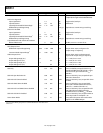
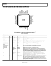
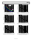
PIN CONFIGURATION AND FUNCTION DESCRIPTIONS
PIN 1
INDICATOR
17
18
19
20
21
22
23
24
25
26
27
28
29
30
31
32
NC
NC
AVDD
NC
NC
NC
AVDD
AVDD
AVDD
AVDD
SYSCLK
SYSCLKB
AVDD
AVDD
LOOP_FILTER
CLKMODESEL
64
63
62
61
60
59
58
57
56
55
54
53
52
51
50
49
SCLK
SDIO
SDO
CSB
IO_UPDATE
RESET
PWRDOWN
DVSS
DVSS
S4
S3
AVDD
AVSS
DAC_OUTB
DAC_OUT
AVDD3
1
2
3
4
5
6
7
8
9
10
11
12
13
14
15
16
DVDD_I/O
DVSS
DVDD
DVSS
DVDD
DVSS
DVDD
DVSS
S1
S2
AVDD
NC
NC
AVDD3
NC
NC
NOTES
1. NC = NO CONNECT.
2. THE EXPOSEDPAD MUST BE CONNECTED TO GROUND FOR PROPER OPERATION.
DAC_RSET
AVDD3
AVDD3
AVDD
AVDD
AVSS
AVDD
FDBK_IN
FDBK_INB
AVSS
OUT_CMOS
AVDD3
AVDD
OUT
OUTB
AVSS
48
47
46
45
44
43
42
41
40
39
38
37
36
35
34
33
06763-002
AD9912
TOP VIEW
(Not to Scale)
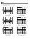
Figure 2. Pin Configuration
Table 5. Pin Function Descriptions
Pin No.
Input/
Output
Pin Type Mnemonic Description
1 I Power DVDD_I/O I/O Digital Supply.
2, 4, 6, 8 I Power DVSS Digital Ground. Connect to ground.
3, 5, 7 I Power DVDD Digital Supply.
9, 10, 54, 55 I/O 3.3 V CMOS S1, S2, S3, S4 Start-Up Configuration Pins. These pins are configured under program
control and do not have internal pull-up/pull-down resistors.
11, 19, 23 to 26,
29, 30, 36, 42, 44,
45, 53
I Power AVDD Analog Supply. Connect to a nominal 1.8 V supply.
12, 13, 15, 16, 17,
18, 20, 21, 22
NC No Connect. These unused pins can be left unconnected.
14, 46, 47, 49 I Power AVDD3 Analog Supply. Connect to a nominal 3.3 V supply.
27 I Differential
input
SYSCLK System Clock Input. The system clock input has internal dc biasing and
should always be ac-coupled, except when using a crystal. Single-ended
1.8 V CMOS can also be used, but it may introduce a spur caused by an input
duty cycle that is not 50%. When using a crystal, tie the CLKMODESEL pin
to AVSS, and connect crystal directly to this pin and Pin 28.
28 I Differential
input
SYSCLKB Complementary System Clock. Complementary signal to the input
provided on Pin 27. Use a 0.01 μF capacitor to ground on this pin if the
signal provided on Pin 27 is single-ended.
31 O LOOP_FILTER System Clock Multiplier Loop Filter. When using the frequency multiplier to
drive the system clock, an external loop filter must be constructed and
attached to this pin. This pin should be pulled down to ground with 1 kΩ
resistor when the system clock PLL is bypassed. See Figure 46 for a diagram
of the system clock PLL loop filter.