


AD9912
Rev. D | Page 2 of 40
TABLE OF CONTENTS
Features .............................................................................................. 1
Applications ....................................................................................... 1
General Description ......................................................................... 1
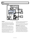
Basic Block Diagram ........................................................................ 1
Revision History ............................................................................... 2
Specifications ..................................................................................... 3
DC Specifications ......................................................................... 3
AC Specifications .......................................................................... 5
Absolute Maximum Ratings ............................................................ 7
Thermal Resistance ...................................................................... 7
ESD Caution .................................................................................. 7
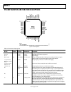
Pin Configuration and Function Descriptions ............................. 8
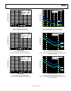
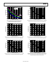
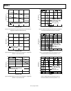
Typical Performance Characteristics ........................................... 10
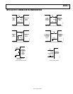
Input/Output Termination Recommendations .......................... 15
Theory of Operation ...................................................................... 16
Overvie w ...................................................................................... 16
Direct Digital Synthesizer (DDS) ............................................. 16
Digital-to-Analog (DAC) Output ............................................ 17
Reconstruction Filter ................................................................. 17
FDBK_IN Inputs ........................................................................ 18
SYSCLK Inputs ........................................................................... 19
Output Clock Drivers and 2× Frequency Multiplier ............. 21
Harmonic Spur Reduction ........................................................ 21
Thermal Performance .................................................................... 23
Power-Up ......................................................................................... 24
Power-On Reset .......................................................................... 24
Default Output Frequency on Power-Up ................................ 24
Power Supply Partitioning ............................................................. 25
3.3 V Supplies .............................................................................. 25
1.8 V Supplies .............................................................................. 25
Serial Control Port ......................................................................... 26
Serial Control Port Pin Descriptions ....................................... 26
Operation of Serial Control Port .............................................. 26
The Instruction Word (16 Bits) ................................................ 27
MSB/LSB First Transfers ........................................................... 27
I/O Register Map ............................................................................ 30
I/O Register Descriptions .............................................................. 32
Serial Port Configuration (Register 0x0000 to
Register 0x0005) ......................................................................... 32
Power-Down and Reset (Register 0x0010 to
Register 0x0013) ......................................................................... 32
System Clock (Register 0x0020 to Register 0x0022) ............. 33
CMOS Output Divider (S-Divider) (Register 0x0100 to
Register 0x0106) ......................................................................... 34
Frequency Tuning Word (Register 0x01A0 to
Register 0x01AD) ....................................................................... 34
Doubler and Output Drivers (Register 0x0200 to
Register 0x0201) ......................................................................... 36
Calibration (User-Accessible Trim) (Register 0x0400 to
Register 0x0410) ......................................................................... 36
Harmonic Spur Reduction (Register 0x0500 to
Register 0x0509) ......................................................................... 36
Outline Dimensions ....................................................................... 38
Ordering Guide .......................................................................... 39
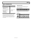
REVISION HISTORY
11/09—Rev. C to Rev. D
Added 64-Lead LFCSP (CP-64-7) .................................... Universal
Changes to Serial Port Timing Specifications and
Propagation Delay Parameters ........................................................ 6
Added Exposed Paddle Notation to Figure 2 ............................... 8
Changes to Power Supply Partitioning Section .......................... 25
Change to Serial Control Port Section ......................................... 26
Changes to Figure 52 ...................................................................... 28
Added Exposed Paddle Notation to Outline Dimensions ........ 38
Changes to Ordering Guide .......................................................... 39
7/09—Rev. B to Rev. C
Changes to Logic Outputs Parameter, Table 1 .............................. 3
Changes to AVDD (Pin 25, Pin 26, Pin 29, and Pin 30) ............ 25
6/09—Rev. A to Rev. B
Changes to Figure 40 and Direct Digital Synthesizer Section .. 17
Changes to Figure 48 ...................................................................... 22
Changes to Table 11 ....................................................................... 30
Changes to Table 22 and Table 23 ................................................ 34
1/08—Rev. 0 to Rev. A
Changes to Table 1 ............................................................................. 3
Changes to Table 2 ............................................................................. 5
Changes to Table 4 ............................................................................. 8
Changes to Typical Performance Characteristics ....................... 10
Changes to Functional Description Section ............................... 19
Changes to Single-Ended CMOS Output Section ..................... 21
Changes to Harmonic Spur Reduction Section ......................... 21
Changes to Power Supply Partitioning Section .......................... 25
10/07—Revision 0: Initial Version