


AD9912
Rev. D | Page 6 of 40
Parameter Min Typ Max Unit Test Conditions/Comments
CMOS Output Driver
(AVDD3/Pin 37) @ 1.8 V
Frequency Range 0.008 40 MHz See Figure 28 for maximum toggle rate
Duty Cycle 45 55 65 % With 20 pF load and up to 40 MHz
Rise Time/Fall Time (20% to 80%) 5 6.8 ns With 20 pF load
DAC OUTPUT CHARACTERISTICS
DCO Frequency Range (1
st
Nyquist Zone) 0 450 MHz DAC lower limit is 0 Hz; however, the minimum slew rate
for FDBK_IN dictates the lower limit if using CMOS or HSTL
outputs
Output Resistance 50 Ω Single-ended (each pin internally terminated to AVSS)
Output Capacitance 5 pF
Full-Scale Output Current 20 31.7 mA Range depends on DAC R
SET
resistor
Gain Error −10 +10 % FS
Output Offset 0.6 μA
Voltage Compliance Range AVSS −
0.50
+0.5 AVSS +
0.50
V Outputs connected to a transformer whose center tap is
grounded
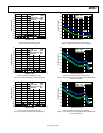
Wideband SFDR See the Typical Performance Characteristics section
20.1 MHz Output −79 dBc 0 MHz to 500 MHz
98.6 MHz Output −67 dBc 0 MHz to 500 MHz
201.1 MHz Output −61 dBc 0 MHz to 500 MHz
398.7 MHz Output −59 dBc 0 MHz to 500 MHz
Narrow-Band SFDR See the Typical Performance Characteristics section
20.1 MHz Output −95 dBc ±250 kHz
98.6 MHz Output −96 dBc ±250 kHz
201.1 MHz Output −91 dBc ±250 kHz
398.7 MHz Output −86 dBc ±250 kHz
DIGITAL TIMING SPECIFICATIONS
Time Required to Enter Power-Down 15 µs
Time Required to Leave Power-Down 18 µs
Reset Assert to High-Z Time
for S1 to S4 Configuration Pins
60 ns Time from rising edge of RESET to high-Z on the S1, S2, S3,
S4 configuration pins
SERIAL PORT TIMING SPECIFICATIONS
SCLK Clock Rate (1/t
CLK
) 25 50 MHz Refer to Figure 56 for all write-related serial port parameters;
maximum SCLK rate for readback is governed by t
DV
SCLK Pulse Width High, t
HIGH
8 ns
SCLK Pulse Width Low, t
LOW
8 ns
SDO/SDIO to SCLK Setup Time, t
DS
1.93 ns
SDO/SDIO to SCLK Hold Time, t
DH
1.9 ns
SCLK Falling Edge to Valid Data on
SDIO/SDO, t
DV
11 ns Refer to Figure 54
CSB to SCLK Setup Time, t
S
1.34 ns
CSB to SCLK Hold Time, t
H
−0.4 ns
CSB Minimum Pulse Width High, t
PWH
3 ns
IO_UPDATE Pin Setup Time
(from SCLK Rising Edge of the Final Bit)
t
CLK
sec t
CLK
= period of SCLK in Hz
IO_UPDATE Pin Hold Time t
CLK
sec t
CLK
= period of SCLK in Hz
PROPAGATION DELAY
FDBK_IN to HSTL Output Driver 2.8 ns
FDBK_IN to HSTL Output Driver with 2×
Frequency Multiplier Enabled
7.3 ns
FDBK_IN to CMOS Output Driver 8.0 ns S-divider bypassed
FDBK_IN Through S-Divider to CMOS
Output Driver
8.6 ns
Frequency Tuning Word Update:
IO_UPDATE Pin Rising Edge to DAC
Output
60/f
S
ns f
S
= system clock frequency in GHz