AD9912
Rev. D | Page 21 of 40
Note that the SYSCLK PLL bypassed and SYSCLK PLL enabled
input paths are internally biased to a dc level of ~1 V. Care should
be taken to ensure that any external connections do not disturb
the dc bias because this may significantly degrade performance.
Generally, it is recommended that the SYSCLK inputs be
ac-coupled, except when using a crystal resonator.
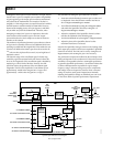
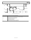
OUTPUT CLOCK DRIVERS AND 2× FREQUENCY
MULTIPLIER
There are two output drivers provided by the AD9912. The
primary output driver supports differential 1.8 V HSTL output
levels, while the secondary supports either 1.8 V or 3.3 V CMOS
levels, depending on whether Pin 37 is driven at 1.8 V or 3.3 V.
The primary differential driver nominally provides an output
voltage with 100 Ω load applied differentially. The source
impedance of the driver is approximately 100 Ω for most of
the output clock period; during transition between levels, the
source impedance reaches a maximum of about 500 Ω. The
driver is designed to support output frequencies of up to and
beyond the OC-12 network rate of 622.08 MHz.
The output clock can also be powered down by a control bit in
the I/O register map.
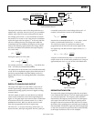
Primary 1.8 V Differential HSTL Driver
The DDS produces a sinusoidal clock signal that is sampled at
the system clock rate. This DDS output signal is routed off chip
where it is passed through an analog filter and brought back on
chip for buffering and, if necessary, frequency doubling. Where
possible, for the best jitter performance, it is recommended that
the frequency doubler be bypassed.
The 1.8 V HSTL output should be ac-coupled, with 100 Ω termi-
nation at the destination. The driver design has low jitter injection
for frequencies in the range of 50 MHz to 750 MHz. Refer to the
AC Specifications section for the exact frequency limits.
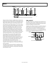
2× Frequency Multiplier
The AD9912 can be configured (via the I/O register map) with
an internal 2× delay-locked loop (DLL) multiplier at the input
of the primary clock driver. The extra octave of frequency gain
allows the AD9912 to provide output clock frequencies that
exceed the range available from the DDS alone. These settings
are found in Register 0x0010 and Register 0x0200.
The input to the DLL consists of the filtered DDS output signal
after it has been squared up by an integrated clock receiver
circuit. The DLL can accept input frequencies in the range of
200 MHz to 400 MHz.
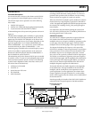
Single-Ended CMOS Output
In addition to the high-speed differential output clock driver,
the AD9912 provides an independent, single-ended output,
CMOS clock driver that is very good for frequencies up to
150 MHz. The signal path for the CMOS clock driver can either
include or bypass the CMOS output divider.
If the CMOS output divider is bypassed, the HSTL and CMOS
drivers are the same frequency as the signal presented at the
FDBK_IN pins. When using the CMOS output in this configu-
ration, the DDS output frequency should be in the range of
30 MHz to 150 MHz. At low output frequencies (<30 MHz), the
low slew rate of the DAC results in a higher noise floor. This can
be remedied by running the DDS at 100 MHz or greater and
using the CMOS divider. At an output frequency of 50 MHz,
the best technique depends on the user’s application. Running
the DDS at 200 MHz, and using a CMOS divider of 4, results in
a lower noise floor, but at the expense of close-in phase noise.
At frequencies greater than 150 MHz, the HSTL output should
be used.
CMOS Output Divider (S-Divider)
The CMOS output divider is 16 bits cascaded with an additional
divide-by-two. The divider is therefore capable of integer division
from 1 to 65,535 (index of 1) or from 2 to 131,070 (index of 2).
The divider is programmed via the I/O register map to trigger
on either the rising (default) or falling edge of the feedback
signal.
The CMOS output divider is an integer divider capable of
handling frequencies well above the Nyquist limit of the DDS.
The S-divider/2 bit (Register 0x0106, Bit 0) must be set when
FDBK_IN is greater than 400 MHz.
Note that the actual output divider values equal the value stored
in the output divider register minus one. Therefore, to have an
output divider of one, the user writes zeros to the output divider
register.
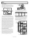
HARMONIC SPUR REDUCTION
The most significant spurious signals produced by the DDS are
harmonically related to the desired output frequency of the DDS.
The source of these harmonic spurs can usually be traced to the
DAC, and the spur level is in the −60 dBc range. This ratio
represents a level that is about 10 bits below the full-scale
output of the DAC (10 bits down is 2
−10
, or 1/1024).
Such a spur can be reduced by combining the original signal
with a replica of the spur, but offset in phase by 180°. This idea
is the foundation of the technique used to reduce harmonic
spurs in the AD9912. Because the DAC has 14-bit resolution,
a −60 dBc spur can be synthesized using only the lower 4 bits of
the DAC full-scale range. That is, the 4 LSBs can create an output
level that is approximately 60 dB below the full-scale level of the
DAC (commensurate with a −60 dBc spur). This fact gives rise
to a means of digitally reducing harmonic spurs or their aliased
images in the DAC output spectrum by digitally adding a sinusoid
at the input of the DAC with a similar magnitude as the offending
spur, but shifted in phase to produce destructive interference.