


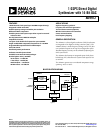

AD9912
Rev. D | Page 7 of 40
ABSOLUTE MAXIMUM RATINGS
Table 3.
Parameter Rating
Analog Supply Voltage (AVDD) 2 V
Digital Supply Voltage (DVDD) 2 V
Digital I/O Supply Voltage
(DVDD_I/O)
3.6 V
DAC Supply Voltage (AVDD3 Pins) 3.6 V
Maximum Digital Input Voltage −0.5 V to DVDD_I/O + 0.5 V
Storage Temperature −65°C to +150°C
Operating Temperature Range −40°C to +85°C
Lead Temperature
(Soldering, 10 sec)
300°C
Junction Temperature 150°C
Stresses above those listed under Absolute Maximum Ratings
may cause permanent damage to the device. This is a stress
rating only; functional operation of the device at these or any
other conditions above those indicated in the operational
section of this specification is not implied. Exposure to absolute
maximum rating conditions for extended periods may affect
device reliability.
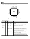
THERMAL RESISTANCE
θ
JA
is specified for the worst-case conditions, that is, a device
soldered in a circuit board for surface-mount packages.
Table 4. Thermal Resistance
Package Type θ
JA
θ
JB
θ
JC
Unit
64-Lead LFCSP 25.2 13.9 1.7 °C/W typical
Note that the exposed pad on the bottom of package must be
soldered to ground to achieve the specified thermal performance.
See the Typical Performance Characteristics section for more
information.
ESD CAUTION