


AD9912
Rev. D | Page 18 of 40
PRIMARY
SIGNAL
FILTER
RESPONSE
SIN(x)/x
ENVELOPE
SPURS
IMAGE 0 IMAGE 1 IMAGE 2 IMAGE 3 IMAGE 4
0
–20
–40
–60
–80
–100
MAGNITUDE
(dB)
f
s
/2
f
s
3
f
s
/2 2
f
s
5
f
s
/2
f
BASE BAND
06763-034
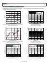
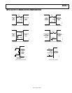
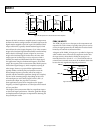
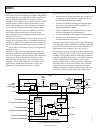
Figure 42. DAC Spectrum vs. Reconstruction Filter Response
Because the DAC constitutes a sampled system, its output must
be filtered so that the analog waveform accurately represents the
digital samples supplied to the DAC input. The unfiltered DAC
output contains the (typically) desired baseband signal, which
extends from dc to the Nyquist frequency (f
S
/2). It also contains
images of the baseband signal that theoretically extend to infinity.
Notice that the odd images (shown in Figure 42) are mirror
images of the baseband signal. Furthermore, the entire DAC
output spectrum is affected by a sin(x)/x response, which is
caused by the sample-and-hold nature of the DAC output signal.
For applications using the fundamental frequency of the DAC
output, the response of the reconstruction filter should preserve
the baseband signal (Image 0), while completely rejecting all
other images. However, a practical filter implementation
typically exhibits a relatively flat pass band that covers the
desired output frequency plus 20%, rolls off as steeply as
possible, and then maintains significant (though not complete)
rejection of the remaining images. Depending on how close
unwanted spurs are to the desired signal, a third
-, fifth-, or
seventh-order elliptic low-p
ass filter is common.
Some applica
tions operate off an image above the Nyquist
frequency, and those applications use a band-pass filter instead
of a low-pass filter.
The design of the reconstruction filter has a significant impact
on the overall signal performance. Therefore, good filter design
and implementation techniques are important for obtaining the
best possible jitter results.
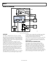
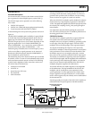
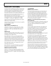
FDBK_IN INPUTS
The FDBK_IN pins serve as the input to the comparators and
output drivers of the AD9912. Typically, these pins are used to
receive the signal generated by the DDS after it has been band-
limited by the external reconstruction filter.
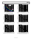
A diagram of the FDBK_IN input pins is provided in Figure 43,
which includes some of the internal components used to bias
the input circuitry. Note that the FDBK_IN input pins are
internally biased to a dc level of ~1 V. Care should be taken to
ensure that any external connections do not disturb the dc bias
because this may significantly degrade performance.
06763-035
15kΩ
15kΩ~1pF
~1pF
TO S-DIVIDER
AND CLOCK
OUTPUT SECTION
AVSS
~1V
AVSS
~2pF
+
FDBK_IN
FDBK_INB
Figure 43. Differential FDBK_IN Inputs