


AD9912
Rev. D | Page 30 of 40
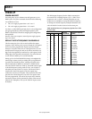
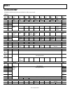
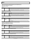
I/O REGISTER MAP
All address and bit locations that are left blank in Table 12 are unused.
Table 12.
Addr
(Hex) Type
1
Name Bit 7 Bit 6 Bit 5 Bit 4 Bit 3 Bit 2 Bit 1 Bit 0
Default
(Hex)
Serial port configuration and part identification
0x0000
Serial
config.
SDO
active
LSB first
(buffered)
Soft
reset
Long
instruction
Long
instruction
Soft reset
LSB first
(buffered)
SDO
active
0x18
0x0001 Reserved 0x00
0x0002 RO Part ID Part ID 0x02
0x0003 RO 0x09
0x0004
Serial
options
Read buffer
register
0x00
0x0005 AC
Register
update
0x00
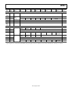
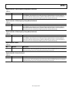
Power-down and reset
0x0010
Power-
down and
enable
PD HSTL
driver
Enable
CMOS
driver
Enable
output
doubler
PD
SYSCLK
PLL
Full PD Digital PD
0xC0 or
0xD0
0x0011 Reserved 0x00
0x0012 M, AC Reset DDS reset 0x00
0x0013 M
PD fund
DDS
S-div/2
reset
S-divider
reset
0x00
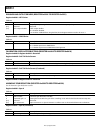
System clock
0x0020
N-divider
N-divider, Bits[4:0]
0x12
0x0021
Reserved
0x00
0x0022
PLL
parameters
VCO auto
range
2× refer-
ence
VCO range
Charge pump current,
Bits[1:0]
0x04
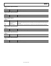
CMOS output divider (S-divider)
0x0100
Reserved
0x30
0x0101
to
0x0103
Reserved
0x00
0x0104
and
0x0105
S-divider
S-divider, Bits[15:0]
LSB: Register 0x0104
0x00
0x0106
Falling
edge
triggered
S-divider/2
0x01
Frequency tuning word
0x01A0
to
0x01A5
Reserved 0x00
0x01A6 M
FTW0
(frequency
tuning
word)
FTW0, Bits[47:0]
LSB: Register 0x01A6
0x00
0x01A7 M 0x00
0x01A8 M 0x00
0x01A9 M 0x00
0x01AA M
Start-up
cond.
0x01AB M
Start-up
cond.
0x01AC M Phase DDS phase word, Bits[7:0] 0x00
0x01AD M DDS phase word, Bits[13:8] 0x00
Doubler and output drivers
0x0200 HSTL driver
OPOL
(polarity)
HSTL output doubler,
Bits[1:0]
0x05
0x0201 CMOS driver CMOS mux 0x00